Image sensor module and formation method thereof
An image sensor and image sensing technology, which is applied in semiconductor/solid-state device manufacturing, electrical components, circuits, etc., to achieve the effect of improving yield rate, high yield rate, and mild process conditions
- Summary
- Abstract
- Description
- Claims
- Application Information
AI Technical Summary
Problems solved by technology
Method used
Image
Examples
Embodiment Construction
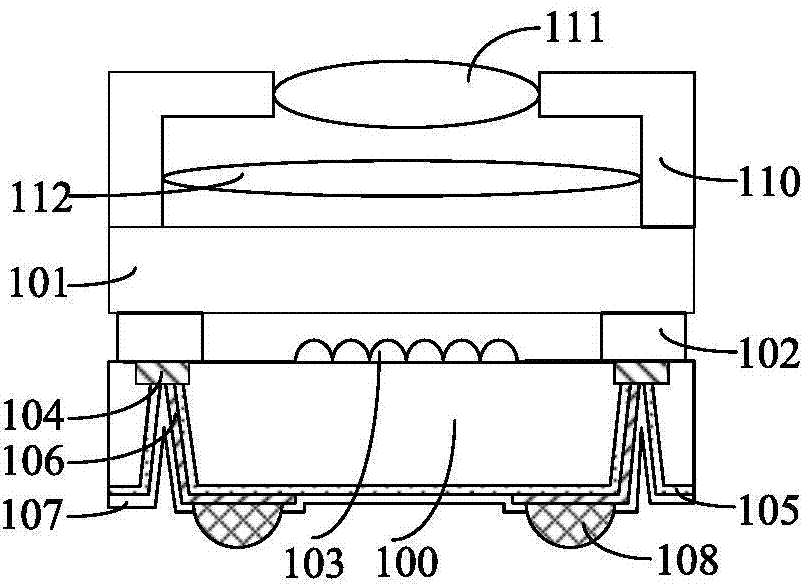
[0049] It can be seen from the background art that the packaging performance and reliability of the image sensor module formed in the prior art need to be further improved, and the process is more complicated and the packaging cost is higher.
[0050] After research, it is found that the packaging performance and reliability of the image sensor module need to be improved because of:
[0051] The packaging process for forming the aforementioned image sensor module is extremely complicated, and the grains are formed by cutting the wafer to be packaged (image sensor chip to be packaged) after a series of packaging processes; the wafer to be packaged undergoes thinning and etching to form through holes , forming a protective layer, forming a metal layer, forming an insulating layer and other multi-channel packaging processes, the packaging process has a negative impact on the performance of the wafer to be packaged, so the performance of the crystal grains formed by cutting the waf...
PUM
 Abstract
Description
Claims
Application Information


