Monolithic Ceramic Electronic Component

一种电子部件、层叠型的技术,应用在固定电容的零部件、电气元件、叠层电容器等方向,能够解决部件功能下降、水分浸入、金属被膜与部件本体固定力弱等问题,达到提高耐湿可靠性、增强接合力的效果

Active Publication Date: 2014-08-06
MURATA MFG CO LTD
View PDF4 Cites 7 Cited by
  • Summary
  • Abstract
  • Description
  • Claims
  • Application Information

AI Technical Summary

Problems solved by technology

[0005] However, as for the metal film formed by direct plating on the predetermined surface of the component body, glass or the like is not used as in the case of forming electrodes by sintering the conductive paste mentioned above, so the metal film first exists. The problem of weak fixing force with the part body
In addition, if the fixing force is weak, cracks may occur at the interface between the metal film and the part body, and moisture will enter from there.
Furthermore, when the intrusion of moisture advances to the interface between the ceramic layer and the internal electrodes, an electrical short occurs between internal electrodes of different potentials through moisture, which may lead to a decrease in the function of the component.

Method used


Image

  • Monolithic Ceramic Electronic Component
  • Monolithic Ceramic Electronic Component
  • Monolithic Ceramic Electronic Component

Examples


Embodiment 1

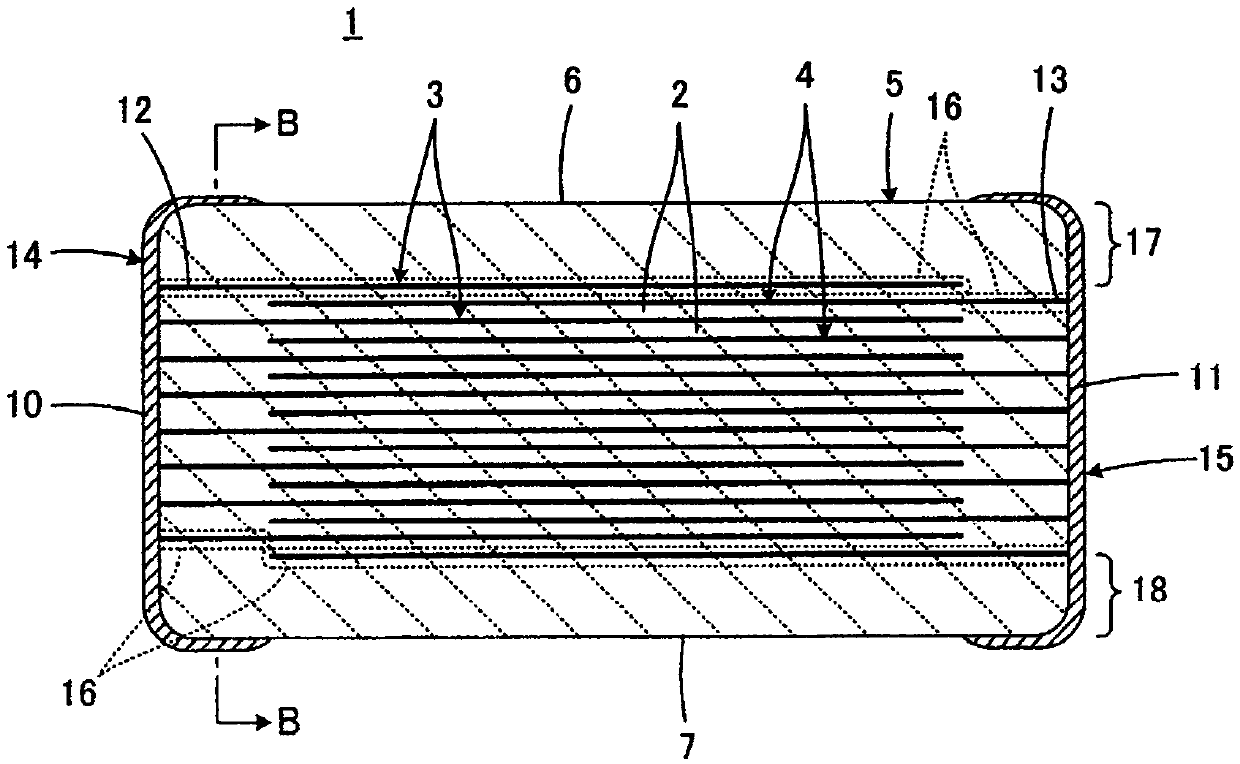
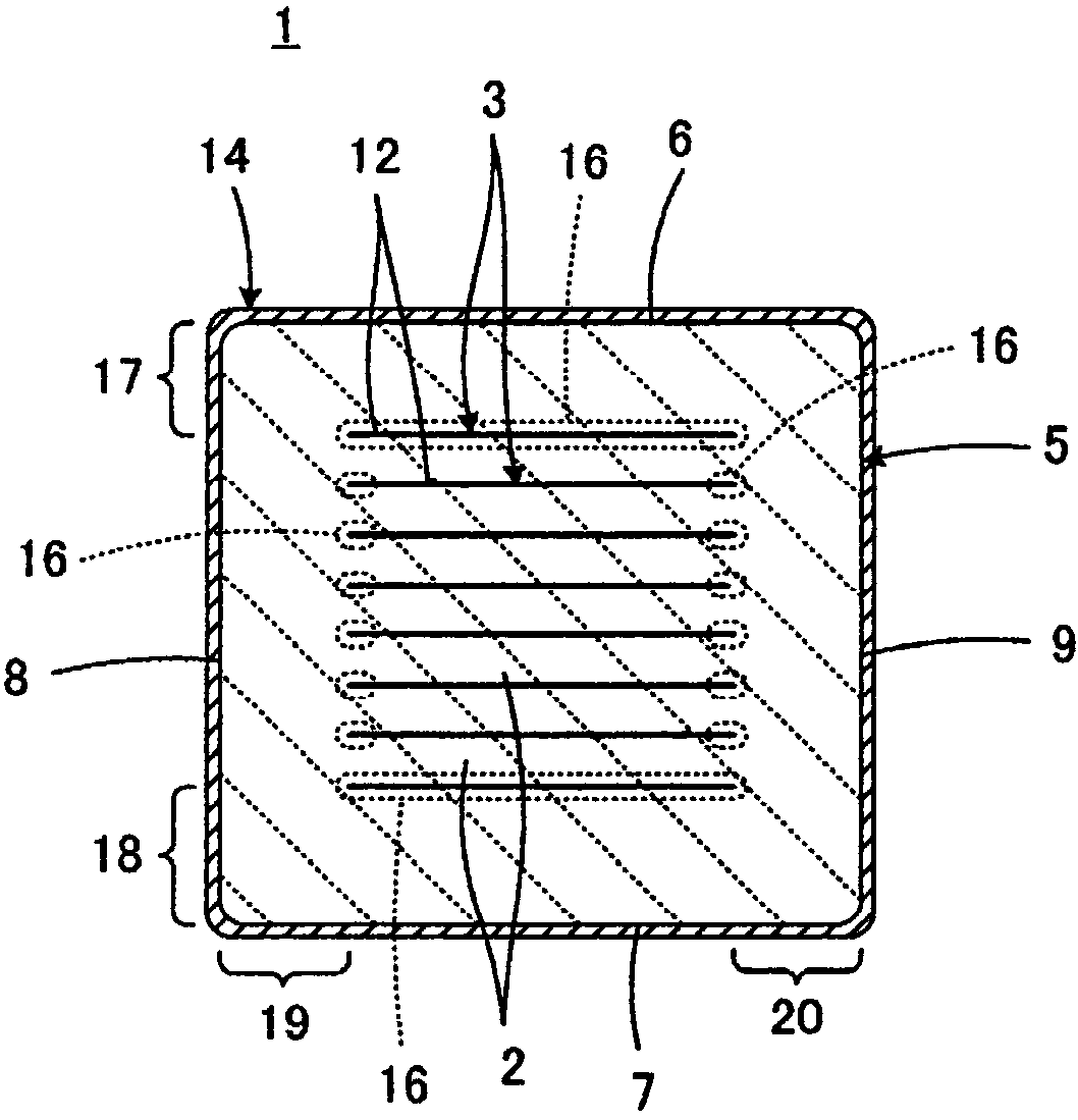
[0049] In Example 1, the effects of the Mg-Ni coexistence region 16 in which the Mg-Ni coexistence region 16 exists were confirmed by focusing particularly on image 3 The portions of the shown first internal electrodes 3 and second internal electrodes 4 that are located in the outer peripheral portion of the region where the exposed ends 12 and 13 are distributed.

[0050] As samples, the following multilayer ceramic electronic components were fabricated.

[0051] First, in order to obtain a component body included in a multilayer ceramic electronic component, an unprocessed component body having ceramic green sheets to be used as a ceramic layer and a Ni-containing layer to be used as an internal electrode is laminated. The structure obtained by the conductive paste film. A barium titanate-based dielectric ceramic raw material to which Mg was added was used as the ceramic raw material contained in the ceramic green sheet.

[0052] Next, the above-mentioned unprocessed comp...

Embodiment 2

[0066] In Example 2, the effects of the Mg-Ni coexistence region 16 in which the Mg-Ni coexistence region 16 exists in the figure 2 Among the regions where the illustrated plurality of first internal electrodes 3 and second internal electrodes 4 are distributed, the outermost first internal electrodes 3 and second internal electrodes 4 are located when viewed in the stacking direction.

[0067] As a sample, a multilayer ceramic electronic component different from that of Example 1 in that it was not an LW inversion type was produced.

[0068] First, a raw component body having the same composition as in the case of Example 1 was prepared. Next, the unprocessed part body is fired. In this sintering step, the oxidizing atmosphere in the heating process before sintering of the ceramic green sheet is controlled, thereby obtaining a sintered component body in which the amount of Mg diffused into the internal electrodes is varied in various ways. The amount of Mg was determined b...

Embodiment 3

[0080] In Example 3, in the same manner as in Example 2, the Mg-Ni coexistence region 16 in which the Mg-Ni coexistence region 16 exists in the figure 2 Among the regions where the illustrated plurality of first internal electrodes 3 and second internal electrodes 4 are distributed, the outermost first internal electrodes 3 and second internal electrodes 4 are located when viewed in the stacking direction.

[0081] As a sample, a multilayer ceramic electronic component was prepared. The multilayer ceramic electronic component was manufactured by electrolytic Cu plating on the component body, followed by electrolytic Ni plating, and then electrolytic Sn plating to form external electrodes. It was manufactured by the same method as in the case of Example 2 except that.

[0082] And, as shown in Table 3, similarly to the case of Example 2, the "region where Mg / Ni=0.1 or more in the outermost layer" and the "peeling occurrence rate" were obtained.

[0083] [table 3]

[0084] ...


PUM


Abstract

A monolithic ceramic electronic component includes a component body and outer electrodes. The component body includes a plurality of stacked ceramic layers and a plurality of inner electrodes which extend between the ceramic layers, which contain Ni, and which include exposed ends exposed on predetermined surfaces of the component body. The outer electrodes are electrically connected to the exposed ends of the inner electrodes and are formed on the predetermined surfaces of the component body by plating. The inner electrodes include Mg—Ni coexistence regions where Mg and Ni coexist.

Description

technical field [0001] The present invention relates to a multilayer ceramic electronic component, and more particularly to a multilayer ceramic electronic component that includes an internal electrode containing Ni and forms an external electrode electrically connected to the internal electrode by plating. Background technique [0002] The external electrodes of a multilayer ceramic capacitor, which is an example of a multilayer ceramic electronic component, are usually formed by applying a conductive paste to the end of the component body and firing it. However, the external electrodes formed by this method have a thickness as high as several tens of μm to several hundreds of μm. Therefore, in order to limit the size of the multilayer ceramic capacitor to a certain standard value, it is necessary to secure the volume of the external electrodes, and it is not desirable to reduce the effective volume for securing the electrostatic capacity. [0003] As a method that can sol...

Claims


Application Information

Patent Timeline
Patent Type & Authority Applications(China)
IPC IPC(8): H01G4/30H01G4/005
CPCH01G4/008H01G4/232H01G4/30H01G4/12H01G4/0085
Inventor 笹林武久元木章博小川诚
Owner MURATA MFG CO LTD
Why Eureka
Try Eureka