Stack type image sensor manufacturing method

An image sensor and stacking technology, which is applied in the field of stacked image sensor preparation, can solve the problems of affecting the output image quality, long process cycle, cumbersome steps, etc., and achieve the effects of improving image output quality, reducing production costs, and simplifying process steps

Active Publication Date: 2014-08-06
OMNIVISION TECH (SHANGHAI) CO LTD
View PDF3 Cites 17 Cited by
  • Summary
  • Abstract
  • Description
  • Claims
  • Application Information

AI Technical Summary

Problems solved by technology

[0005] Continue to refer to figure 1 , as shown in the figure, since the filter layer 400 of the traditional stacked CMOS image sensor is arranged on the metal grid 600 and spaced apart from the metal grid 600, a series of processes must be performed after the metal grid 600 is prepared Steps, such as depositing an oxide layer to cover the metal gate 600, performing a series of subsequent preparation processes such as planarization, the steps are relatively cumbersome, the process cycle is long and the cost is also high
[0006] At the same time, when the devi

Method used


Image

  • Stack type image sensor manufacturing method
  • Stack type image sensor manufacturing method
  • Stack type image sensor manufacturing method

Examples


Embodiment 1

[0061] This embodiment provides a method for a stacked image sensor, and the specific steps are as follows:

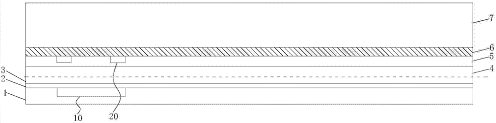
[0062] Step S1: providing a semiconductor device, the semiconductor device includes a logic wafer (logic wafer) and a device wafer (pixel wafer, or pixel wafer) bonded on the logic wafer, the logic wafer is embedded with a second A metal electrode, a second metal electrode is embedded in the device wafer.

[0063] Specifically, firstly, a logic wafer and a device wafer are provided, and the device wafer is bonded on the upper surface of the logic wafer. Wherein, both the logic wafer and the device wafer are provided with multi-layer oxide layers, and a silicon layer is provided on the top of the device wafer, and the first metal electrode is embedded in one of the oxide layers of the logic wafer, and includes the The upper surface of the oxide layer of the first metal electrode is covered with a mask layer, and the second metal electrode is embedded in one of the oxid...

Embodiment 2

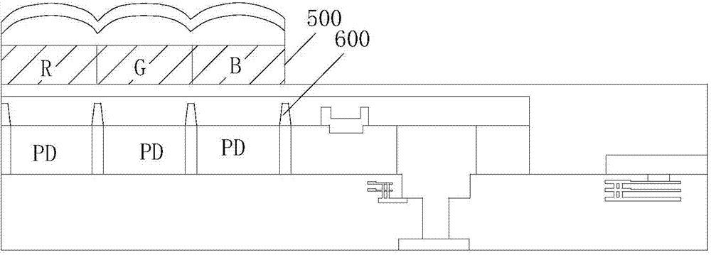
[0076]Based on the first embodiment above, the present application also provides a stacked image sensor prepared by the above preparation method, including a filter layer and a metal grid, and the filter layer is embedded in the metal grid, and can be combined with conventional Other device structures together form a stacked image sensor, that is, in this embodiment, by embedding the filter layer in the metal grid, the crosstalk phenomenon in the PD layer can be effectively avoided, thereby improving the output quality of the image , and compared with the traditional device structure, its preparation process can be greatly simplified to reduce its production cost, and it can be widely used in electronic image equipment such as mobile phones, digital cameras, and DVs.

Embodiment 3

[0078] This embodiment provides a method for preparing a stacked image sensor, and the specific steps are as follows:

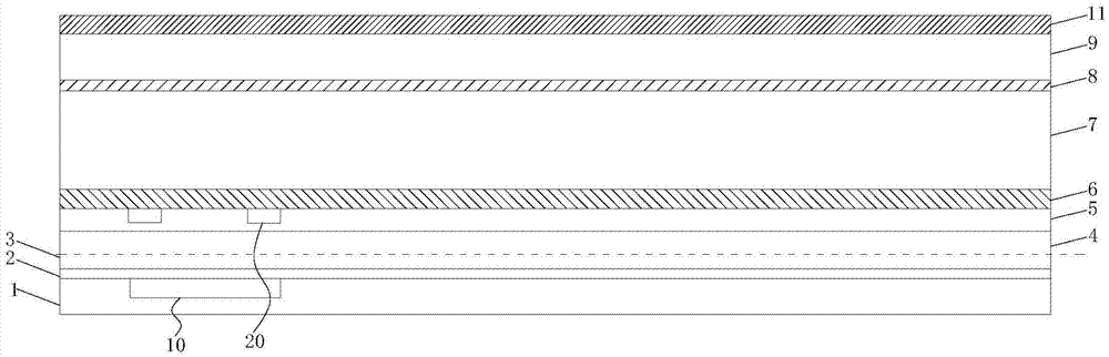
[0079] Step S1: Provide a semiconductor device for preparing a stacked image sensor, the semiconductor device includes a logic wafer (logic wafer) and a device wafer (pixel wafer, or pixel wafer) bonded on the logic wafer , the first metal electrode is embedded in the logic wafer, and the second metal electrode is embedded in the device wafer.

[0080] Specifically, firstly, a logic wafer and a device wafer are provided, and the device wafer is bonded on the upper surface of the logic wafer. Wherein, both the logic wafer and the device wafer are provided with multi-layer oxide layers, and the top of the device wafer is also provided with a silicon layer, and the first metal electrode is embedded in one of the oxide layers of the logic wafer, and The upper surface of the oxide layer including the first metal electrode is covered with a mask layer, and the sec...


PUM


Abstract

The invention provides a stack type image sensor manufacturing method. As a filtering layer is embedded into a metal grid, when being compared with a conventional technique, in the method, a great number of unnecessary steps is omitted, the machine utilization rate is increased, and the production cost is reduced, and meanwhile, by adopting an image sensor manufactured by using the method, the influence of crosstalk to an image is effectively alleviated, and furthermore the quality of an output image is improved.

Description

technical field [0001] The invention relates to the field of image sensor preparation, in particular to a method for preparing a stacked image sensor. Background technique [0002] CMOS image sensor belongs to optoelectronic components. CMOS image sensor has gradually become the mainstream of image sensor because its manufacturing process is compatible with the existing integrated circuit manufacturing process, and its performance has many advantages over the original charge-coupled device (CCD) image sensor. . The CMOS image sensor can integrate the driving circuit and the pixel together, which simplifies the hardware design and reduces the power consumption of the system at the same time. The CMOS image sensor can take out the electrical signal while collecting the optical signal, and can also process the image information in real time, which is faster than the CCD image sensor. At the same time, the CMOS image sensor also has the advantages of cheap price, large bandwidt...

Claims


Application Information

Patent Timeline
IPC IPC(8): H01L27/146
Inventor 高喜峰施喆天叶菁刑家明
Owner OMNIVISION TECH (SHANGHAI) CO LTD
Why Eureka
Try Eureka