JFET (junction field-effect transistor) device and manufacturing method thereof

A device and substrate technology, which is applied in the field of JFET devices and its manufacturing, can solve the problems of not being able to meet the application of constant current source circuits and low cost, and achieve the effect of good constant current characteristics and small constant current accuracy

Inactive Publication Date: 2014-08-06
UNIV OF ELECTRONICS SCI & TECH OF CHINA
View PDF4 Cites 3 Cited by
  • Summary
  • Abstract
  • Description
  • Claims
  • Application Information

AI Technical Summary

Problems solved by technology

Its driving circuit has a simple structure and extremely low cost, and the core of providing constant current is a normally-on n-channel JFET device, but the current conventional JFET device cannot well meet the application of constant current source circuit

Method used


Image

  • JFET (junction field-effect transistor) device and manufacturing method thereof
  • JFET (junction field-effect transistor) device and manufacturing method thereof
  • JFET (junction field-effect transistor) device and manufacturing method thereof

Examples


Embodiment 1

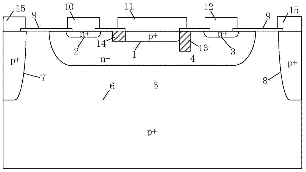
[0037] In this example, a shallow trench auxiliary layer is formed by digging a trench and filling a dielectric material layer, specifically:

[0038] Step 1: Select an NTD single wafer with fewer defects. The thickness of the single wafer ranges from 400 to 700 μm, and the resistivity ranges from 0.001 to 0.005Ω·cm. After marking, cleaning, and drying, it is ready to use, such as Figure 6 shown;

[0039] Step 2: grow an epitaxial layer on the surface of the silicon wafer, the temperature range is 1100 ° C ~ 1150 ° C, the thickness is 5 ~ 25 μ m, and the resistivity is 8 ~ 12 Ω·cm, such as Figure 7 shown;

[0040] Step 3: Thermally grow oxide layer with a thickness of

[0041] The fourth step: a photolithography, after the photolithography, the P+ isolation region is implanted, and the first P-type isolation region and the second P-type isolation region are formed on both sides of the epitaxial layer, such as Figure 8 Shown; Specifically, the glue-removing implant is u...


PUM


Abstract

The invention relates to semiconductor technology, particularly a JFET (junction field-effect transistor) device and a manufacturing method thereof. A current shallow groove auxiliary layer (13) and a voltage shallow groove auxiliary layer (14) are introduced into the ditch of the JFET device; the current shallow groove auxiliary layer (13) and voltage shallow groove auxiliary layer (14) are positioned on both ends of a P+ gate region (1) and connected with the P+ gate region (1); the current shallow groove auxiliary layer (13) is utilized to reduce the ditch modulation effect, thereby implementing small variable rate of output current within wide voltage input range; and the combined action of the voltage shallow groove auxiliary layer (14) and current shallow groove auxiliary layer (13) is utilized to reduce the curvature effect, thereby enhancing the voltage resistance of the device. The device has favorable constant-current characteristic on the basis of uncomplex manufacturing technique, has small variable rate within wide voltage input range, can satisfy the demand for lower constant-current precision, and is especially suitable for low-power LED (light-emitting diode) lamp constant-current drive. The method is especially suitable for low-power LED lamp constant-current JFET devices.

Description

technical field [0001] The invention relates to semiconductor technology, in particular to a JFET device and a manufacturing method thereof. Background technique [0002] With the widespread use of LED lamps, LED constant current drivers are rapidly occupying the market. The constant current JFET device is a constant current driver designed for low-power LEDs. It can achieve constant current output in a wide voltage range from 4V to 150V, and It can achieve ±15% constant current accuracy, can be matched with LED lamp beads, and is widely used in indoor lighting. figure 1 It is a solution for driving LEDs with constant current. Due to the high output voltage, this solution is especially suitable for LED applications with a current value of 5mA to 500mA, especially for high-voltage LEDs. The scheme includes a total of 6 components, simple and practical, and low cost. figure 1 Among them, the AC mains directly drives the constant current device and the LED light string after ...

Claims


Application Information

Patent Timeline
Patent Type & Authority Applications(China)
IPC IPC(8): H01L29/78H01L29/10H01L21/336H01L21/265
CPCH01L29/808H01L29/1058H01L29/66893
Inventor 李泽宏赖亚明刘建吴玉舟
Owner UNIV OF ELECTRONICS SCI & TECH OF CHINA
Why Eureka
Try Eureka