Shift register unit, grid driving circuit and display device

A shift register and gate technology, applied in the fields of gate drive circuits, display devices, and shift register units, can solve problems such as high power consumption, and achieve the effect of solving large power loss losses

Active Publication Date: 2014-08-13
BOE TECH GRP CO LTD +1
View PDF5 Cites 29 Cited by
  • Summary
  • Abstract
  • Description
  • Claims
  • Application Information

AI Technical Summary

Problems solved by technology

[0004] The embodiment of the present invention provides a shift register unit, a gate drive circuit and a display device, which are used to solve the problem c

Method used


Image

  • Shift register unit, grid driving circuit and display device
  • Shift register unit, grid driving circuit and display device
  • Shift register unit, grid driving circuit and display device

Examples


Embodiment 1

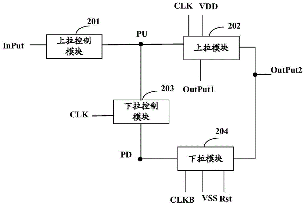
[0024] Such as figure 2 As shown, it is a schematic structural diagram of the shift register unit in Embodiment 1 of the present invention. The shift register unit includes: a pull-up control module 201, a pull-up module 202, a pull-down control module 203, and a pull-down module 204, wherein:

[0025] The pull-up control module 201, whose input terminal is connected to the transmission signal input terminal, and whose output terminal is connected to the pull-up node, is used to output the pull-up control signal to the pull-up node PU according to the transmission signal input by the transmission signal input terminal. The pull node PU is located on the wire used to connect the pull-up control module and the pull-up module;

[0026] The pull-up module 202, whose input terminal is connected to the pull-up node, and whose output terminal is connected to the gate drive signal output terminal and the transmission signal output terminal, is used to input the first clock signal inp...

Embodiment 2

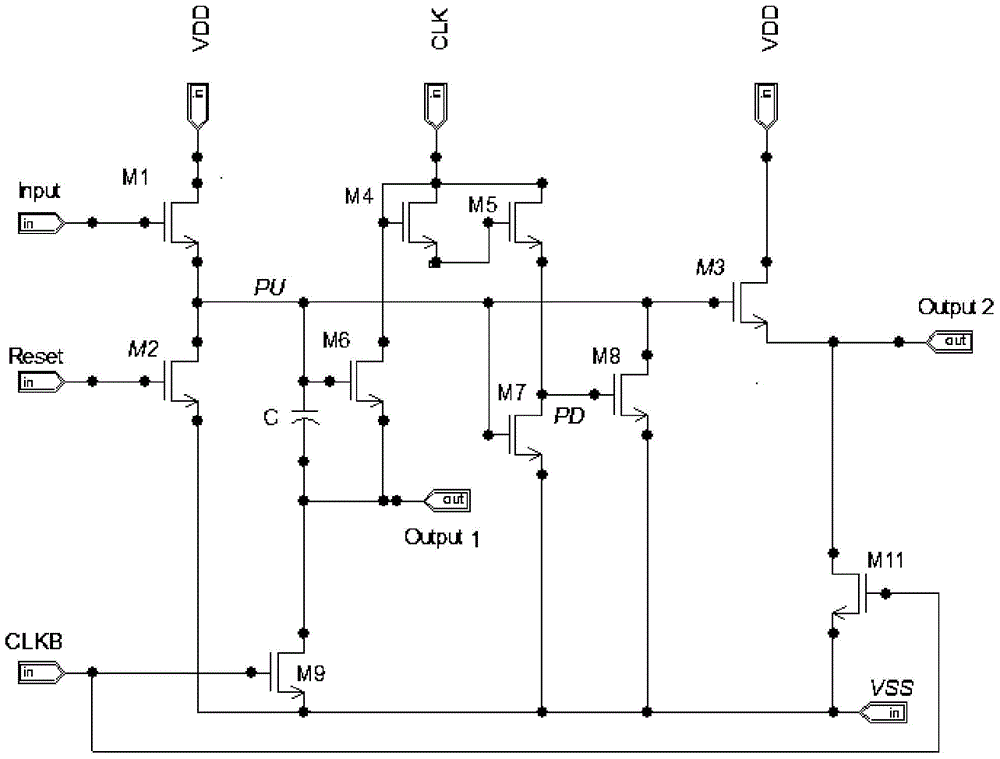
[0041] Such as image 3 Shown is a schematic circuit diagram of the shift register unit in Embodiment 2 of the present invention. in:

[0042] The signals input to the shift register unit include: the first clock signal CLK, the second clock signal CLKB, the transfer signal InPut, the reset signal Reset, the first DC power supply voltage VDD (always a high level signal) and the second DC power supply Voltage signal VSS (always a low-level signal); the signals output from the shift register unit include: transfer signal Output1 and gate drive signal Output2;

[0043] In addition, the pull-up module 202 is formed by the capacitor C, the sixth transistor M6, and the third transistor M3;

[0044] The first pull-down sub-module in the first mode in Embodiment 1 is formed by the second transistor M2 and the eighth transistor M8;

[0045] The second pull-down sub-module in the first mode in Embodiment 1 is formed by the eleventh transistor M11;

[0046] The third pull-down sub-mo...

Embodiment 3

[0089] Based on the same inventive concept as that of Embodiment 1 and Embodiment 2 of the present invention, Embodiment 3 of the present invention provides a gate drive circuit, the schematic diagram of which is shown in Figure 6 As shown, the gate drive circuit includes a plurality of shift register units as described in Embodiment 1: S / R(1), S / R(2)...S / R(N), a total of N shift register units Register unit, except for the first shift register unit and the last shift register unit, the transfer signal output terminals of each shift register unit are connected To the reset signal input terminal of the upper shift register unit adjacent to it and the transfer signal input terminal of the next shift register unit adjacent to it, the gate drive circuit sequentially outputs the gates of the shift register units of each level The gate drive signal output by the pole drive signal output terminal;

[0090] The transfer signal output terminal of the first shift register unit is conn...


PUM


Abstract

The invention discloses a shift register unit, a grid driving circuit and a display device. Specifically, the shift register unit comprises a pull-up control module, a pull-up module, a pull-down control module and a pull-down module; the pull-up module provides a first clock signal to a transmission signal output terminal according to a pull-up control signal and provides first direct-current supply voltage to a grid driving signal output terminal according to the pull-up control signal and the first clock signal, wherein the first clock signal is input by a first clock signal input terminal. Due to the fact that the first direct-current supply voltage is used as input of a transistor, used for outputting grid driving signals, in the pull-up module, the transistor has no capacity coupling effects, namely, due to the fact that high and low level conversion does not exist in the first direct-current supply voltage, stray capacitance generated by the transistor cannot be charged or discharged frequently, power losses are reduced and the problem that power consumption of a common shift register unit is high is solved.

Description

technical field [0001] The invention relates to the field of flat panel display technology, in particular to a shift register unit, a gate drive circuit and a display device. Background technique [0002] Such as figure 1 Shown is a schematic circuit diagram of a shift register unit in the prior art. The shift register unit includes a pull-up control module composed of a first transistor M1, a pull-up module composed of a third transistor M3 and a capacitor C, a pull-up module composed of a second transistor M2, a fourth transistor M4, a tenth transistor M10 and a tenth transistor A pull-down module composed of a transistor M11 and a pull-down control module composed of a fifth transistor M5, a sixth transistor M6, a ninth transistor M9 and an eighth transistor M8. Signal input terminal input signal (INPUT), first clock signal input terminal input first clock signal (CLK), second clock signal input terminal (CLKB) input second clock signal (CLKB), low voltage signal input ...

Claims


Application Information

Patent Timeline
IPC IPC(8): G09G3/20G09G3/36G11C19/28
CPCG09G3/36G11C19/28G09G2310/0286G09G2330/021
Inventor 李金钰
Owner BOE TECH GRP CO LTD
Why Eureka
Try Eureka