Poly-silicon thin film transistor and preparation method thereof, and array substrate

A polysilicon thin film and transistor technology, which is applied in the direction of transistors, semiconductor/solid-state device manufacturing, electric solid-state devices, etc., can solve problems affecting the performance of thin-film transistors, large leakage current, inconsistent length, etc.

Active Publication Date: 2014-08-20
BOE TECH GRP CO LTD +1
View PDF3 Cites 20 Cited by
  • Summary
  • Abstract
  • Description
  • Claims
  • Application Information

AI Technical Summary

Problems solved by technology

[0012] However, during this process, the inventors found that before performing light doping, the photoresist in the semi-retained part 402 of the photoresist needs to be removed by an ashing process in S104, and the exposed gate metal film needs to be Wet etching is carried out, and both the wet etching and ashing processes a

Method used


Image

  • Poly-silicon thin film transistor and preparation method thereof, and array substrate
  • Poly-silicon thin film transistor and preparation method thereof, and array substrate
  • Poly-silicon thin film transistor and preparation method thereof, and array substrate

Examples


Embodiment Construction

[0034] The following will clearly and completely describe the technical solutions in the embodiments of the present invention with reference to the accompanying drawings in the embodiments of the present invention. Obviously, the described embodiments are only some, not all, embodiments of the present invention. Based on the embodiments of the present invention, all other embodiments obtained by persons of ordinary skill in the art without making creative efforts belong to the protection scope of the present invention.

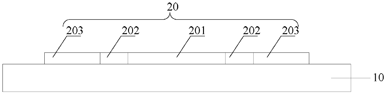
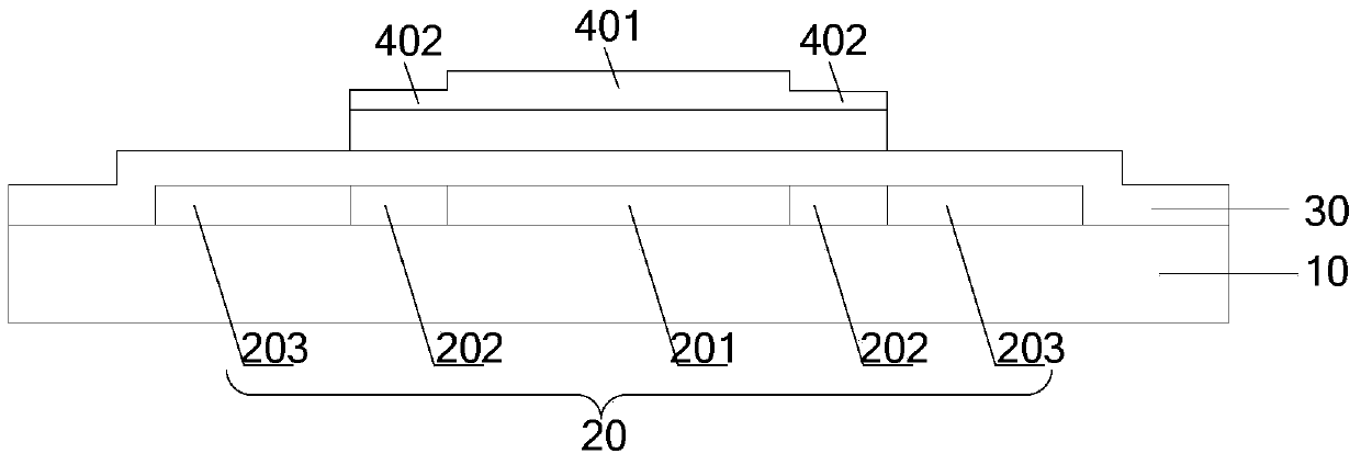
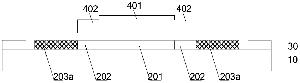
[0035] An embodiment of the present invention provides a method for preparing a polysilicon thin film transistor, comprising: forming an active layer, a gate insulating layer above the active layer, a gate electrode, a source electrode, and a drain electrode on a base substrate; The active layer includes a first polysilicon region, a lightly doped region located on both sides of the first polysilicon region, and a heavily doped region located on a side of the l...


PUM


Abstract

The embodiment of the invention provides a poly-silicon thin film transistor and a preparation method thereof, and an array substrate, and relates to the technical field of display. Lightly doped regions can be made consistent in length, and the problem of too large leakage current can be avoided. According to the thin film transistor, an active layer, a gate insulation layer, a gate electrode, a source electrode and a drain electrode are formed on a substrate base plate, and the active layer comprises a first poly-silicon region, lightly doped regions disposed on the two sides of the first poly-silicon region, and heavily doped regions disposed on one sides of the lightly doped regions. According to the method, dry etching is performed to form a barrier layer between the gate electrode and the gate insulation layer, wherein the barrier layer corresponds to the first poly-silicon region. The formation of the lightly doped regions of the active layer comprises the following steps: a poly-silicon layer is formed on the substrate base plate, wherein the poly-silicon layer includes a first poly-silicon region, second poly-silicon regions disposed on the two sides of the first poly-silicon region, and third poly-silicon regions disposed on one sides of the second poly-silicon regions; and the second poly-silicon regions are doped to form the lightly doped regions with the use of the barrier layer covering the first poly-silicon region as a mask.

Description

technical field [0001] The invention relates to the field of display technology, in particular to a polysilicon thin film transistor, a preparation method thereof, and an array substrate. Background technique [0002] Low Temperature Poly-Silicon-Thin Film Transistor (LTPS-TFT) display has the advantages of high resolution, fast response, high brightness, high aperture ratio, etc., and due to the characteristics of LTPS, it has high In addition, the peripheral driving circuit can also be fabricated on the glass substrate at the same time, so as to achieve the goal of system integration, save space and cost of driving IC, and reduce the defective rate of products. [0003] At present, the preparation method of the low-temperature polysilicon thin film field effect transistor includes the following steps: [0004] S101, such as figure 1 As shown, a polysilicon layer 20 is formed on the base substrate 10, and the polysilicon layer 20 includes: the first polysilicon region 201...

Claims


Application Information

Patent Timeline
IPC IPC(8): H01L29/786H01L21/336H01L27/12
CPCH01L29/66757H01L21/28088H01L27/1262H01L27/1288H01L29/4966H01L29/66492H01L29/7833H01L29/78621H01L29/78675H01L29/6675H01L27/1214H01L29/78672
Inventor 姜晓辉张家祥
Owner BOE TECH GRP CO LTD
Why Eureka
Try Eureka