Manufacturing method for nitride LED assembly

A technology of light-emitting diodes and nitrides, which is applied in the direction of electrical components, semiconductor devices, circuits, etc., can solve the problems of reduced crystal quality of the P-type semiconductor layer, large damage to the light-emitting layer, and affecting luminous performance, so as to reduce the efficiencydroop effect and increase the recombination Efficiency, the effect of enhancing luminous efficiency

Active Publication Date: 2014-08-20
TIANJIN SANAN OPTOELECTRONICS
View PDF4 Cites 8 Cited by
  • Summary
  • Abstract
  • Description
  • Claims
  • Application Information

AI Technical Summary

Problems solved by technology

[0003] Since the growth temperature of the MQW light-emitting layer of the InGaN LED structure is generally 750-850°C, the growth temperature of the P-type semiconductor layer is relatively high, generally 900-1000°C, but the higher the temperature of the P-type semiconductor layer, the greater the damage to the light-emitting layer, resulting in The recombination efficiency is low, which affects th

Method used


Image

  • Manufacturing method for nitride LED assembly
  • Manufacturing method for nitride LED assembly

Examples


Embodiment

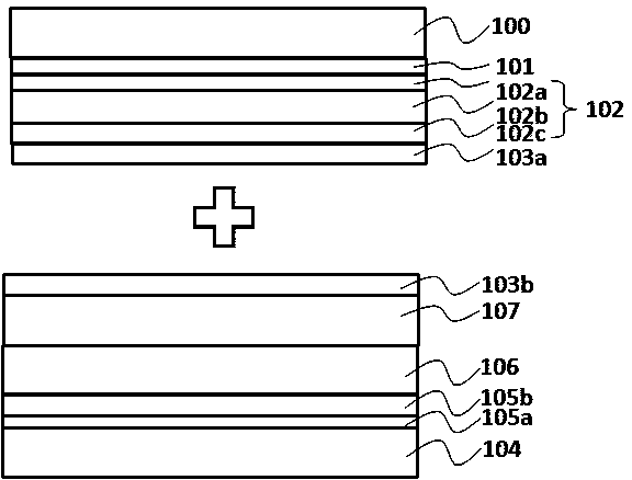
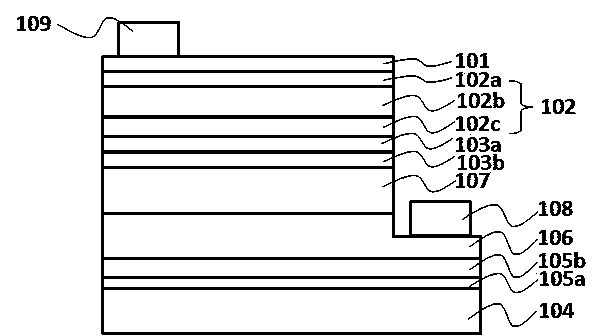
[0026] like figure 1 and 2 As shown, a method for preparing a nitride light-emitting diode assembly, the method is realized by the following steps:

[0027] (1) Provide a transition substrate 100, the transition substrate is selected from alumina single crystal (Sapphire) or SiC (6H-SiC or 4H-SiC) or Si or GaAs or GaN or a combination thereof, preferably in this embodiment Si substrate;

[0028] (2) Form a transparent conductive layer 101 on the transition substrate 100. The transparent conductive layer can be ITO, IZO, ZnO, GZO, ITO containing silicon oxide, etc., and ITO is preferred in this embodiment;

[0029] (3) Growing a P-type semiconductor layer 102 and a first GaN layer 103a sequentially on the transparent conductive layer 101, wherein the P-type semiconductor layer includes a P-type contact layer, a P-type layer and an electron blocking layer, and the first GaN layer 103a has a thickness of 1-100nm, preferably 10nm;

[0030] (4) Provide a permanent substrate 10...


PUM


Abstract

The invention relates to a manufacturing method for a nitride LED assembly. The method has the advantages of reducing electron leakage, relieving the efficiencydroop effect, increasing hole concentration and enhancing light-emitting efficiency. The method is implemented by the adoption of the steps that (1) a transition substrate is provided; (2) a P-type semiconductor layer and a first bonding layer sequentially grow on the transition substrate; (3) a permanent substrate is provided; (4) a N-type semiconductor layer, a light-emitting layer and a second bonding layer sequentially grow on the permanent substrate; (5) the transition substrate where the P-type semiconductor layer grows and the permanent substrate where the N-type semiconductor layer and the light-emitting layer grow are bonded through the first bonding layer and the second bonding layer.

Description

technical field [0001] The invention relates to a nitride semiconductor optoelectronic device, in particular to a method for preparing a nitride light-emitting diode assembly. Background technique [0002] In recent years, light-emitting diode (LED for short) components have focused on improving brightness, and are expected to be applied in the lighting field to play the role of energy saving and carbon reduction. In general, traditional InGaN LED components include: a nitride buffer layer formed on a sapphire substrate, an n-type contact layer doped with GaN by Si, and a multi-layer quantum well structure with InGaN (Multi-Quantum- The light-emitting layer of Well (MQW for short) is a structure formed by stacking Mg-doped AlGaN electron blocking layer and Mg-doped p-type nitride contact layer in sequence. This structure has the characteristics of semiconductor components with high brightness. [0003] Since the growth temperature of the MQW light-emitting layer of the InGa...

Claims


Application Information

Patent Timeline
IPC IPC(8): H01L33/00
CPCH01L33/005H01L33/007H01L33/0075H01L33/06H01L33/32H01L33/0093H01L33/00H01L33/12H01L33/62H01L2933/0066
Inventor 董木森申利莹王笃祥王良均刘晓峰
Owner TIANJIN SANAN OPTOELECTRONICS
Why Eureka
Try Eureka