
Method for detecting abnormity of mechanical arm of detector

A robotic arm and inspection machine technology, applied in semiconductor/solid-state device testing/measurement, electrical components, circuits, etc., can solve the problem of inability to effectively monitor the abnormal changes of the robotic arm in real time, and achieve the effect of ensuring yield

Inactive Publication Date: 2014-09-03
SHANGHAI HUALI MICROELECTRONICS CORP
View PDF7 Cites 3 Cited by
  • Summary
  • Abstract
  • Description
  • Claims
  • Application Information

AI Technical Summary

Problems solved by technology

[0008] The present invention solves the problem that the existing technology cannot effectively monitor the subtle abnormal changes of the mechanical arm in real time, thereby providing a technical solution for detecting the abnormality of the mechanical arm of the machine

Method used


Image

  • Method for detecting abnormity of mechanical arm of detector
  • Method for detecting abnormity of mechanical arm of detector
  • Method for detecting abnormity of mechanical arm of detector

Examples


Embodiment Construction

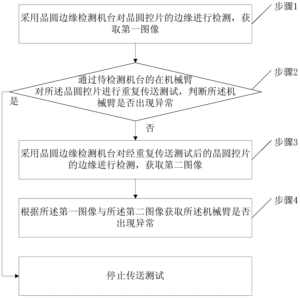
[0031] The present invention will be further described below in conjunction with the accompanying drawings and specific embodiments, but not as a limitation of the present invention.

[0032] Such as Figures 1 to 8 As shown, the present invention provides a method for detecting an abnormality of a machine arm, comprising the following steps:

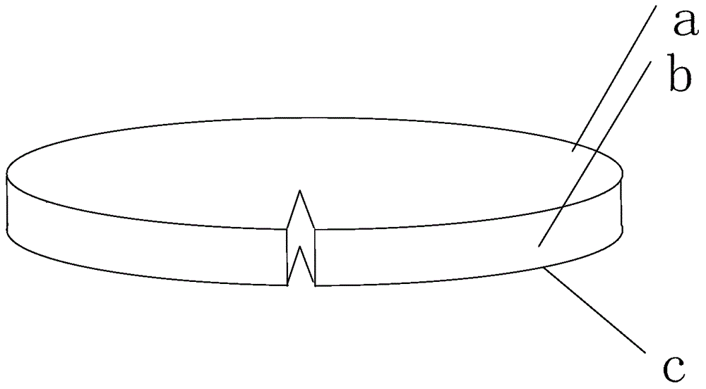
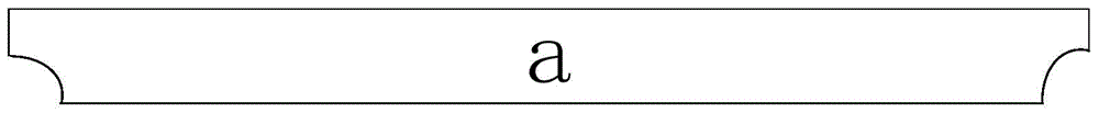
[0033] Step 1. Use a wafer edge detection machine to detect the edge of the wafer control sheet, and obtain the first image (such as image 3 , Figure 5 and Figure 7 As shown in the first image of upper surface edge a, side b and lower surface edge c), a low-resistance material layer is grown on the outer surface of the wafer control chip, and the thickness of the low-resistance material layer is a fixed value;

[0034] Step 2. Repeat the transfer test on the wafer control piece through the robot arm of the machine to be tested (that is, place the wafer control piece in the machine to be tested and perform a repeated delivery test ...


PUM


Abstract

The invention discloses a method for detecting abnormity of a mechanical arm of a detector, relating to the semiconductor field. The method comprises the steps that 1) the wafer edge detector detects the edge of a control wafer to obtain a first image; 2) a transmission test is repeatedly carried out on the control wafer via the mechanical arm of the detector to be detected to determine whether the mechanical arm is abnormal, if yes, the transmission test is stopped, and if no, a step 3) is implemented; 3) the wafer edge detector detects the edge of the control wafer after repeated transmission tests to obtain a second image; and 4) whether the mechanical arm is abnormally is determined according to the first and second images. The method can be used to effectively monitor working states of the mechanical arm in real time, if the mechanical arm is detected to be abnormal, the mechanical arm can be further inspected timely and effectively, and thus, the yield rate of products is ensured.

Description

technical field [0001] The invention relates to the field of semiconductors, in particular to a method for detecting the edge of a wafer control chip by using a wafer edge detection machine to obtain abnormality of a mechanical arm. Background technique [0002] With the continuous improvement of integrated circuit technology, more and more chips can be produced per unit area, and the wafer size is getting larger and larger. The precision requirements for production machines are also gradually increasing, especially in terms of the mechanical arm of the machine. Once there is a problem with the accuracy of the mechanical arm, it is very easy to cause abnormal contact between the wafer and the mechanical arm, resulting in scratch defects, and further caused by scratches. The induced grain defects cause defects in the normal chip product area of ​​the wafer. At present, in order to ensure the normal operation and stability of the robotic arm in wafer production enterprises, t...

Claims


Application Information

Patent Timeline
IPC IPC(8): H01L21/66
CPCH01L22/10
Inventor 朱陆君倪棋梁龙吟陈宏璘
Owner SHANGHAI HUALI MICROELECTRONICS CORP
Features
  • Generate Ideas
  • Intellectual Property
  • Life Sciences
  • Materials
  • Tech Scout
  • Unparalleled Data Quality
  • Higher Quality Content
  • 60% Fewer Hallucinations
Learn More