Semiconductor structure and forming method thereof

A semiconductor and forming layer technology, which is applied in the direction of semiconductor devices, semiconductor/solid device manufacturing, semiconductor/solid device components, etc., can solve problems such as poor electrical performance, delamination, electromigration failure, etc., to improve adhesion, Effect of avoiding delamination, improving yield and electrical performance

Active Publication Date: 2014-09-03
SEMICON MFG INT (SHANGHAI) CORP
View PDF5 Cites 5 Cited by
  • Summary
  • Abstract
  • Description
  • Claims
  • Application Information

AI Technical Summary

Problems solved by technology

[0004] However, when conducting the wiring bonding test (Wiring bonding test) on the above-mentioned copper interconnection structure, it was found that the barrier layer 106 in the copper interconnection structure is easily peeled off from the in

Method used


Image

  • Semiconductor structure and forming method thereof
  • Semiconductor structure and forming method thereof
  • Semiconductor structure and forming method thereof

Examples


Embodiment Construction

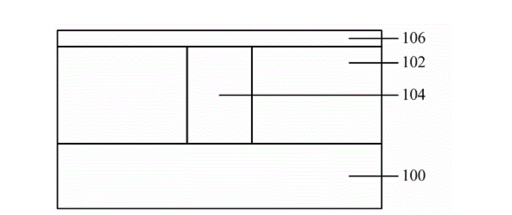
[0035] As mentioned in the background technology section, in the copper interconnection structure formed by the existing technology, the barrier layer is easily peeled off from the interlayer dielectric layer and the copper interconnection line, the yield of the formed copper interconnection structure is low, and electromigration is prone to occur invalidated.

[0036] The inventors have found through research that the barrier layer in the copper interconnection structure is easy to peel off from the interlayer dielectric layer and the copper interconnection because: the copper interconnection is a conductive material, the barrier layer is an insulating material, and the copper interconnection and the barrier layer Poor adhesion due to different materials, resulting in the barrier layer being easily peeled off from the copper interconnect. Similarly, when an insulating layer is formed on a metal layer of other materials, the above-mentioned problems must also exist.

[0037] ...


PUM

PropertyMeasurementUnit
Thicknessaaaaaaaaaa
Thicknessaaaaaaaaaa

Abstract

A semiconductor structure and a forming method thereof are provided; the semiconductor structure comprises the following elements: a semiconductor substrate; an interlayer dielectric layer positioned on the semiconductor substrate; a metal layer positioned in the interlayer dielectric layer; a bonding layer positioned on the metal layer; a stop layer positioned on the interlayer dielectric layer and the bonding layer. A surface of the bonding layer contacting with the metal layer contains conductive material, and a surface of the bonding layer contacting with the stop layer contains insulation material. The method improves bonding property between the metal layer and the stop layer in the semiconductor structure, so the metal layer and the stop layer cannot be disengaged, thereby further improving yield and the electric performance of the semiconductor structure.

Description

technical field [0001] The invention relates to the technical field of semiconductor manufacturing, in particular to a semiconductor structure and a forming method thereof. Background technique [0002] As the production of integrated circuits develops towards ultra-large-scale integrated circuits (ULSI), the internal circuit density is increasing, and the number of components contained is increasing, so that the surface of the wafer cannot provide enough area to make the required interconnection lines (Interconnect). In order to meet the increased demand for interconnection lines after the shrinkage of components, the design of multilayer metal interconnection lines with more than two layers realized by using through holes has become a method that must be adopted in VLSI technology. [0003] Due to the low resistivity of copper metal and long electromigration life, using copper technology to make metal interconnection lines can reduce the RC (Resistive Capacitive delay) de...

Claims


Application Information

Patent Timeline
IPC IPC(8): H01L21/768H01L23/538
CPCH01L21/76841H01L23/522
Inventor 周鸣
Owner SEMICON MFG INT (SHANGHAI) CORP
Why Eureka
Try Eureka