Three-dimensional semiconductor device and manufacturing method thereof

A semiconductor and device technology, applied in the field of three-dimensional semiconductor memory devices and their manufacturing, can solve problems such as low read and write efficiency, inability to perform bulk erasing, etc., to improve device reliability, improve gate threshold voltage control characteristics, and avoid excessive Etching effect

Active Publication Date: 2014-09-03
INST OF MICROELECTRONICS CHINESE ACAD OF SCI
View PDF3 Cites 44 Cited by
  • Summary
  • Abstract
  • Description
  • Claims
  • Application Information

AI Technical Summary

Problems solved by technology

[0007] However, although the BiCS structure uses the control gate threshold by stacking the memory array and the selection transistor, it can only be erased by the gate-induced drain leakage current (GIDL), and cannot be erased by the body, and the read and write efficiency is low.

Method used


Image

  • Three-dimensional semiconductor device and manufacturing method thereof
  • Three-dimensional semiconductor device and manufacturing method thereof
  • Three-dimensional semiconductor device and manufacturing method thereof

Examples


Embodiment Construction

[0027] The features and technical effects of the technical solution of the present invention will be described in detail below with reference to the accompanying drawings and in conjunction with exemplary embodiments, and a semiconductor storage device and a manufacturing method thereof that effectively improve gate control performance and device reliability are disclosed. It should be pointed out that similar reference numerals represent similar structures, and the terms "first", "second", "upper", "lower" and the like used in this application can be used to modify various device structures or manufacturing processes . These modifications do not imply spatial, sequential or hierarchical relationships of the modified device structures or fabrication processes unless specifically stated.

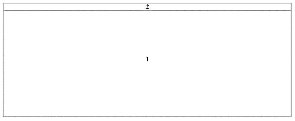
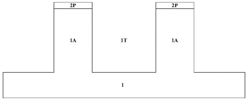
[0028] Figure 1 to Figure 16 A cross-sectional view showing various steps of the method for forming a multi-gate select transistor and forming a storage transistor string thereon by adopting...


PUM


Abstract

The invention discloses a three-dimensional semiconductor device comprising a plurality of memory unit transistors and a plurality of selection transistors, wherein the plurality of memory unit transistors are at least partially overlapped in the vertical direction; each selection transistor comprises a first drain electrode distributed along the vertical direction, an active region, a common source electrode formed in a substrate and a metal grid electrode distributed around the active region; each memory unit transistor comprises a channel layer distributed vertical to the surface of the substrate, wherein a plurality of interlayer insulating layers and a plurality of grid electrode stacking structures are alternately stacked along the side wall of the channel layer, and a second drain electrode is located at the top of the channel layer; the channel layer is electrically connected with the first drain electrode. According to the three-dimensional semiconductor device and a manufacturing method thereof disclosed by the invention, multi-grid MOSFETs (Metal-Oxide-Semiconductor Field Effect Transistors) are formed below memory unit string stacks comprising vertical channels so as to be used as the selection transistors, thus the threshold voltage control characteristic of the grid electrode is improved, the off-state leakage current is reduced, the over-etching for the substrate is avoided, and the reliability of the device is effectively improved.

Description

technical field [0001] The invention relates to a semiconductor device and a manufacturing method thereof, in particular to a three-dimensional semiconductor storage device and a manufacturing method thereof. Background technique [0002] In order to improve the density of memory devices, the industry has made extensive efforts to develop methods of reducing the size of two-dimensionally arranged memory cells. As the size of memory cells in two-dimensional (2D) memory devices continues to shrink, signal collisions and interference can increase significantly, making it difficult to perform multi-level cell (MLC) operations. In order to overcome the limitations of 2D memory devices, the industry has developed memory devices with a three-dimensional (3D) structure to increase integration density by three-dimensionally arranging memory cells on a substrate. [0003] A currently commonly used 3D memory device structure in the industry is a terabit cell array transistor (TCAT). ...

Claims


Application Information

Patent Timeline
Patent Type & Authority Applications(China)
IPC IPC(8): H01L27/115H01L21/8247
CPCH10B41/35H10B41/27H01L29/40117H10B43/27H10B43/35
Inventor 霍宗亮
Owner INST OF MICROELECTRONICS CHINESE ACAD OF SCI
Why Eureka
Try Eureka