Detection device and method for splicing measurement of surface shape using pinhole diffraction wave front

A small hole diffraction and detection device technology, applied in the direction of measuring devices, optical devices, instruments, etc., can solve the problems of reduced measurement resolution and limited detector resolution, and achieve the effect of expanding lateral resolution

Inactive Publication Date: 2014-09-10
INST OF OPTICS & ELECTRONICS - CHINESE ACAD OF SCI
View PDF5 Cites 25 Cited by
  • Summary
  • Abstract
  • Description
  • Claims
  • Application Information

AI Technical Summary

Problems solved by technology

[0016] From the development and application principle of the point diffraction interferometer, it can be seen that the point diffraction interferometer uses the principle of a small hole to generate an ideally diffracted spherical wave for measurement. Due to the limited resolution of the detector, the measurement resolution decreases with the increase of the detection aperture. decrease

Method used


Image

  • Detection device and method for splicing measurement of surface shape using pinhole diffraction wave front
  • Detection device and method for splicing measurement of surface shape using pinhole diffraction wave front
  • Detection device and method for splicing measurement of surface shape using pinhole diffraction wave front

Examples


Embodiment Construction

[0060] In order to make the object, technical solution and advantages of the present invention clearer, the present invention will be described in further detail below in conjunction with specific embodiments and with reference to the accompanying drawings.

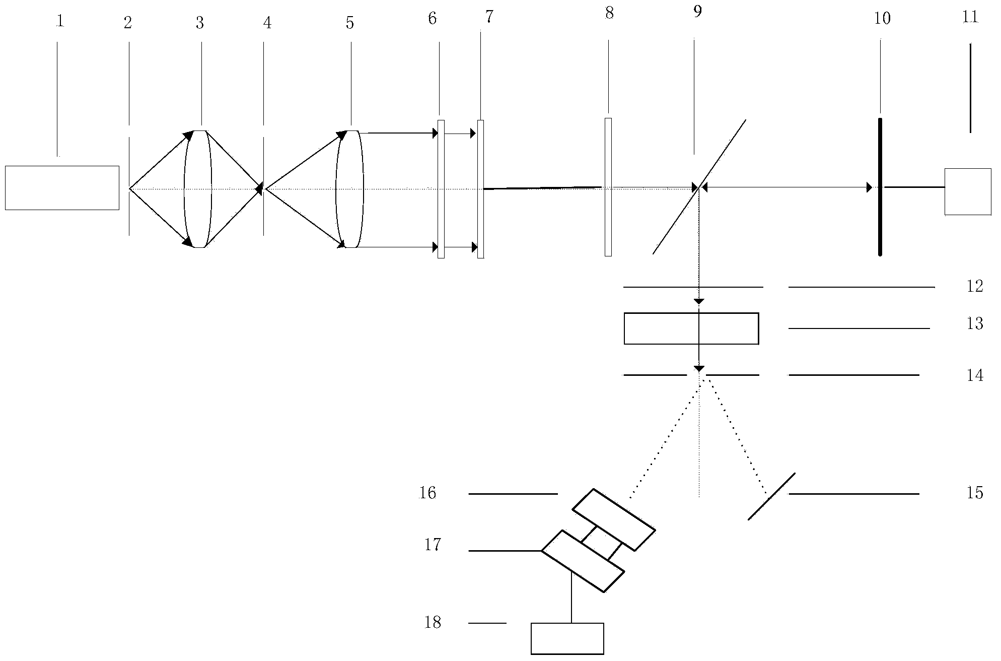
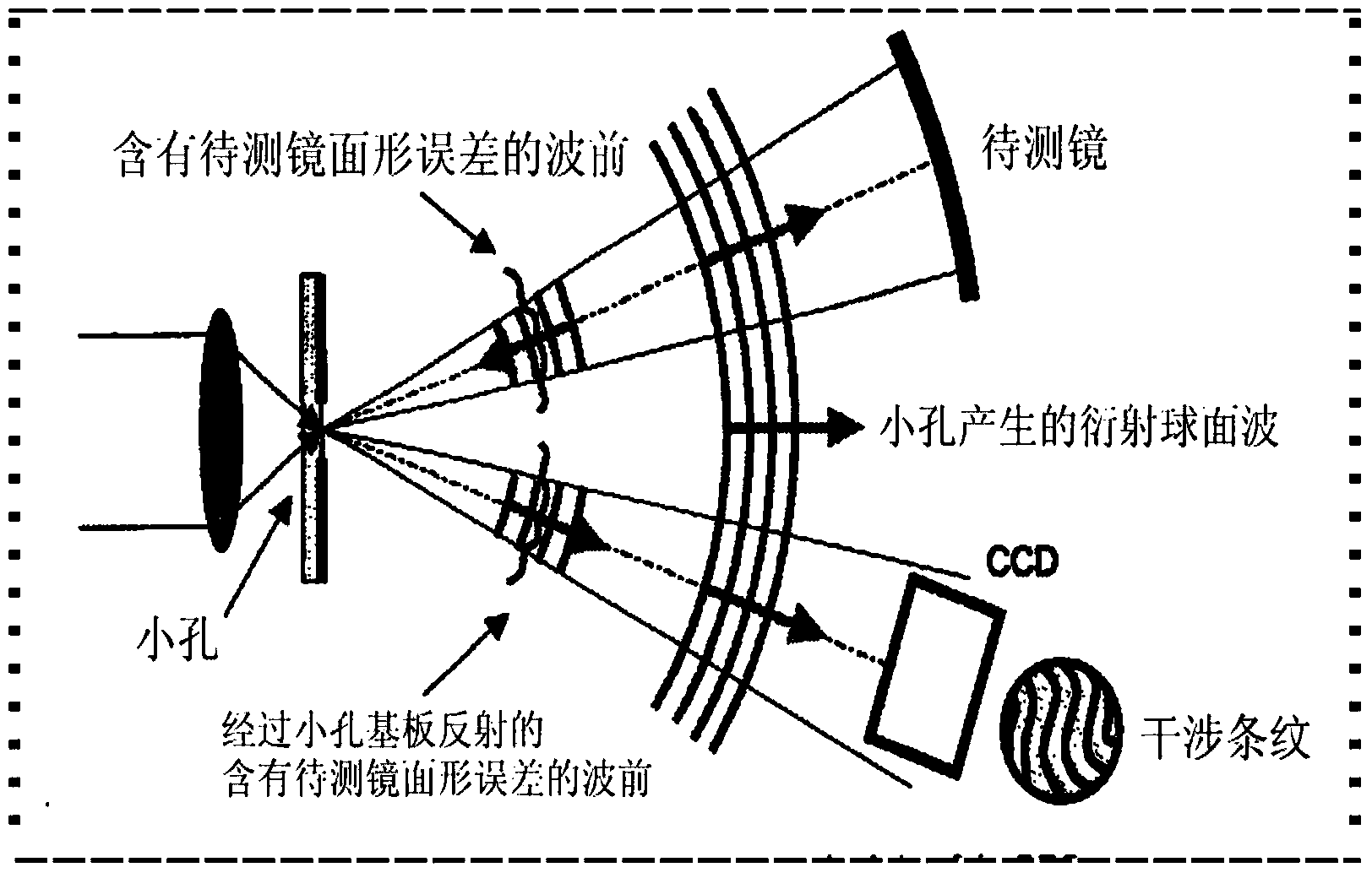
[0061] like figure 1 It shows a schematic structural view of a detection device that utilizes pinhole diffraction wave surface splicing to measure surface shape in the present invention, consisting of a laser 1, a filter hole 2, a first condenser lens 3, a spatial filter 4, a beam expander 5, and a λ / 2 wave plate 6 , λ / 4 wave plate 7, attenuation plate 8, beam splitter 9, reflector 10, phase shifter 11, first optical adjustment mount 12, second condenser lens group 13, aperture substrate 14, second optical adjustment mount 15, The third optical adjustment mount 16, the CCD detector 17 and the computer 18. Among them: the filter hole 2 is placed at the light outlet of the laser 1, the first condenser lens 3 is placed betw...


PUM


Abstract

The invention provides a detection device and method for splicing measurement of a surface shape using pinhole diffraction wave front. Light emitted by a laser passes a filtering hole, a first collecting lens, a spatial filter, a beam expanding mirror, a lambda/2 wave plate, a lambda/4 wave plate, and an attenuation plate to be transmitted by a beam splitter, reflected by a reflection mirror, subsequently reflected by the beam splitter, and irradiated by a first optical adjusting frame and a second collecting lens set into a pinhole. Partial diffraction light produced by the pinhole is irradiated to a mirror surface to be detected, reflected light of the mirror surface to be detected is reflected by a pinhole frame to produce interference fringes with a part of diffraction wave surfaces of the pinhole, and the interference fringes pass s convergence optical unit and then are collected by an optical detector. The mirror surface to be detected is placed on a second optical adjusting frame and can move along a normal direction of the mirror surface to be detected for annular aperture splicing measurement, and meanwhile, rotation and translation of the first optical adjusting frame can be controlled for performing scanning and splicing measurement on the mirror surface to be detected.

Description

technical field [0001] The invention belongs to the technical field of optical surface shape detection, and in particular relates to a detection device and method for measuring surface shape by splicing small hole diffracted wave surfaces. Background technique [0002] The point diffraction interferometer uses small hole diffraction to generate standard reference spherical waves for interferometric measurement. The sub-aperture splicing measurement method is to divide the surface to be measured into sub-apertures for splicing measurement, which can improve the lateral resolution of detection. [0003] The proposal of the Point Diffraction Interferometer (PDI) solves the problem of reference surface processing in high-precision measurement. Its main feature is that it does not use the traditional reference surface, but from the point of view of wave optics, it uses small hole diffraction to generate The ideal reference spherical wave eliminates the limitation of the reference...

Claims


Application Information

Patent Timeline
Patent Type & Authority Applications(China)
IPC IPC(8): G01B11/24
CPCG01B9/02041G01B9/02038G01B11/2441G01B9/02001
Inventor 贾辛许嘉俊徐富超谢伟民邢廷文
Owner INST OF OPTICS & ELECTRONICS - CHINESE ACAD OF SCI
Why Eureka
Try Eureka