Pixel circuit and display device

A technology for pixel circuits and display devices, applied in static indicators, instruments, etc., can solve the problem of uneven display brightness of display devices, reduce the number of signal lines, reduce costs, and solve the effects of threshold voltage drift

Active Publication Date: 2014-09-10
BOE TECH GRP CO LTD +1
View PDF6 Cites 19 Cited by
  • Summary
  • Abstract
  • Description
  • Claims
  • Application Information

AI Technical Summary

Problems solved by technology

[0006] The purpose of the present invention is to solve the problem of uneven display brightness of the display device, reduce the number of signal lines used for the pixel circuit in the display device, reduce the cost of the integrated circuit, and improve the pixel density of the display device at the same time

Method used


Image

  • Pixel circuit and display device
  • Pixel circuit and display device
  • Pixel circuit and display device

Examples


Embodiment Construction

[0031] The specific implementation manners of the present invention will be further described below in conjunction with the drawings and examples. The following examples are only used to illustrate the technical solution of the present invention more clearly, but not to limit the protection scope of the present invention.

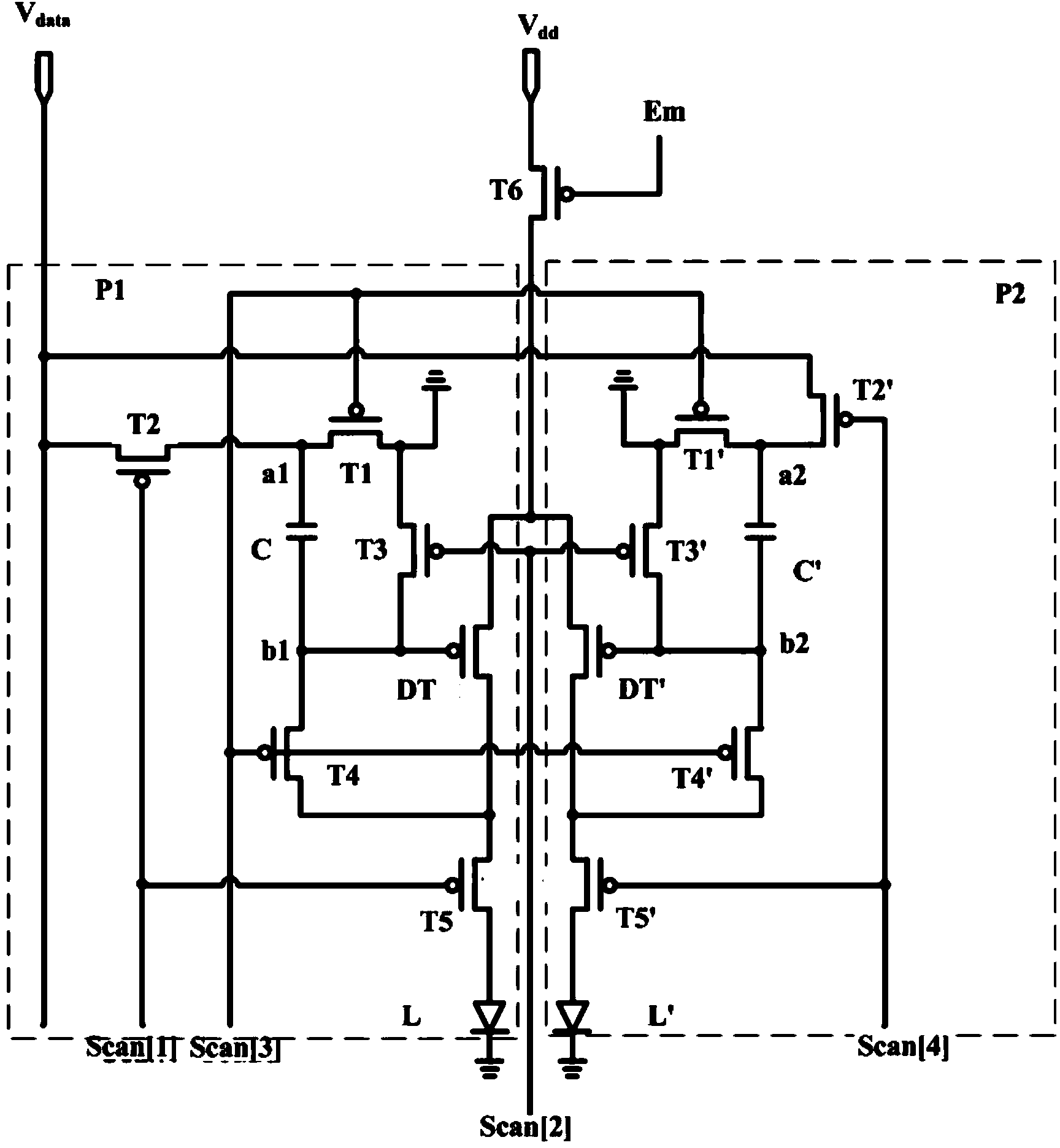
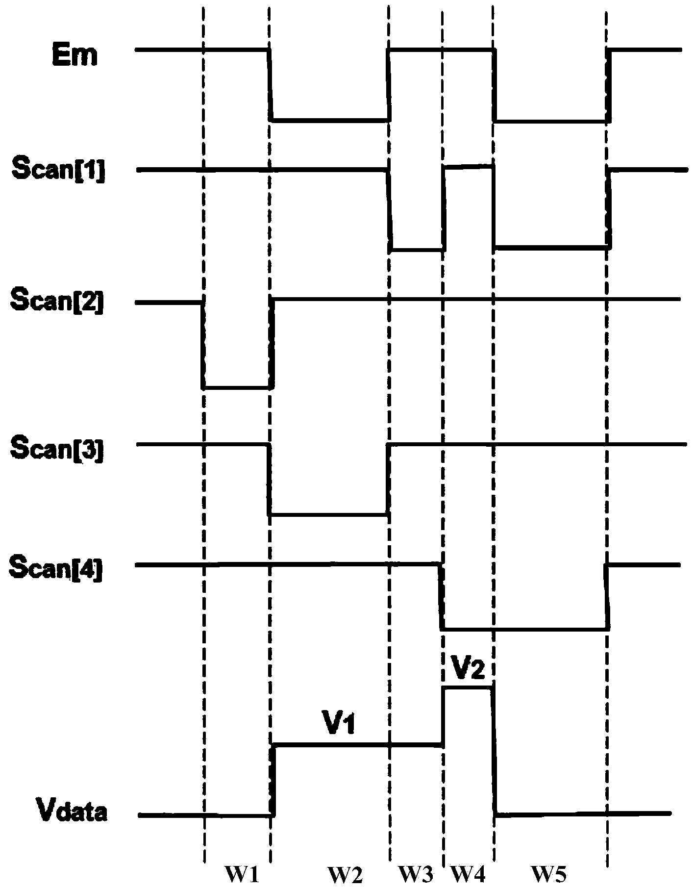
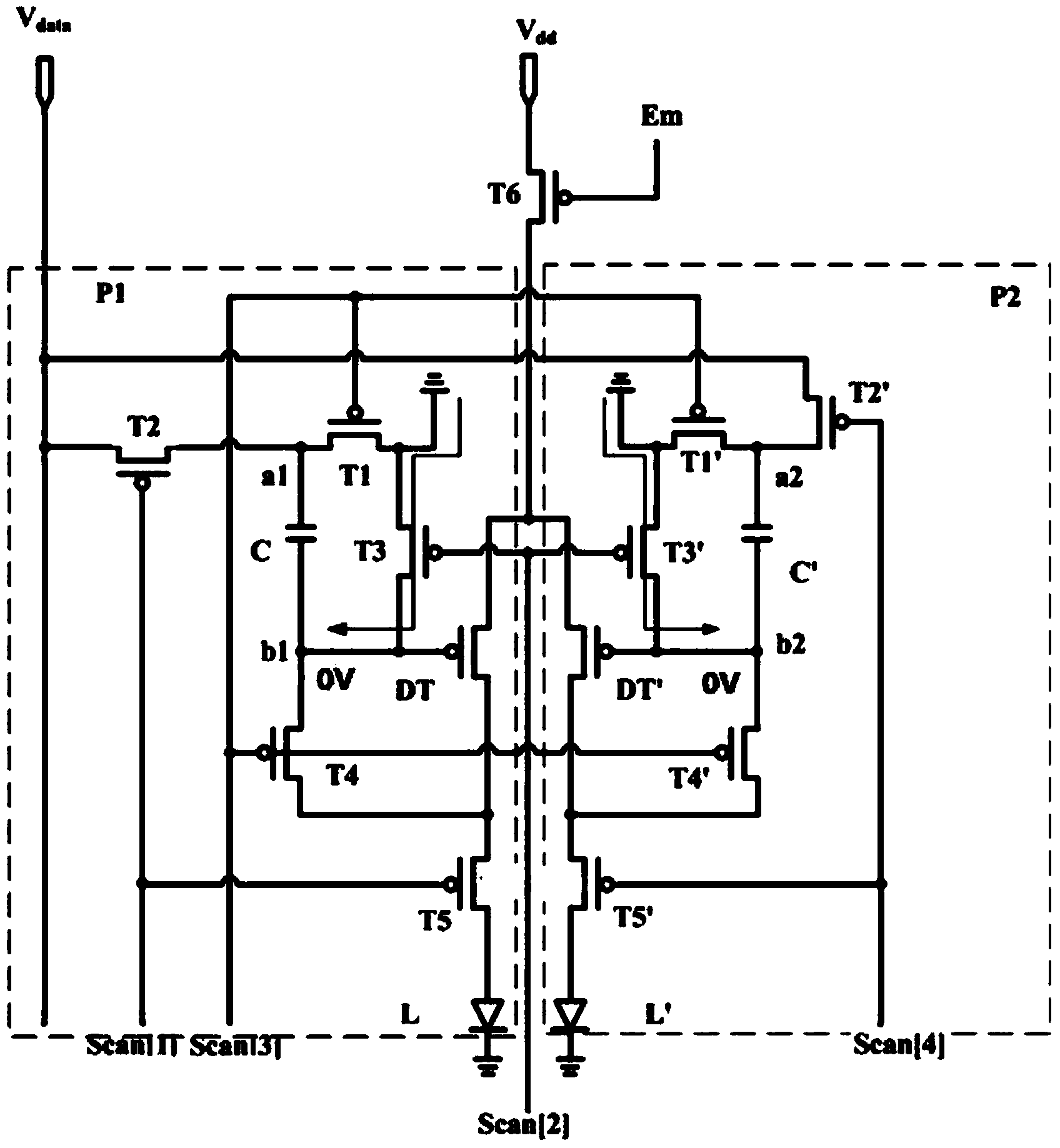
[0032] An embodiment of the present invention provides a pixel circuit, such as figure 1 Or as shown in Figure 3, it includes: two sub-pixel circuits P1 and P2, wherein each pixel sub-circuit includes: five switching units T1, T2, T3, T4, T5, one driving unit DT, one energy storage unit C, one Electroluminescence unit L (for easy distinction, in figure 1 Or in Figure 3, the five switching units in P2 are represented as T1', T2', T3', T4', T5' respectively, the drive unit is represented as DT', the energy storage unit is C', and the electroluminescent unit is L ', the same below),

[0033] And, the first terminal of T1 is connected to the first terminal a...


PUM


Abstract

The invention provides a pixel circuit. The pixel circuit comprises two sub-pixel circuits and a sixth switch unit, wherein the first end of the sixth switch unit is connected to a working voltage line, and the control end is connected to a first scanning signal line; each sub-pixel circuit comprises five switch units, a driving unit, an energy storing unit and an electroluminescent unit; a first switch unit, a third switch unit and a fourth switch unit of the first sub-pixel circuit share the scanning signal line with a first switch unit, a third switch unit and a fourth switch unit of a second sub-pixel circuit. By adopting the pixel circuit, the problem of non-uniform display brightness due to drifting of threshold voltage for driving a transistor is solved completely. Meanwhile, driving of two pixels is finished by using one compensating circuit, and two adjacent pixels share a plurality of signal lines, thereby reducing the quantity of signal lines for the pixel circuit in the display device, lowering the cost of an integrated circuit, reducing pixel distances and increasing the pixel density.

Description

technical field [0001] The present invention relates to the field of display technology, in particular to a pixel circuit and a display device. Background technique [0002] Organic light-emitting display (OLED) is one of the hot spots in the field of flat panel display research. Compared with liquid crystal display, OLED has the advantages of low energy consumption, low production cost, self-illumination, wide viewing angle and fast response speed. Currently, OLEDs have begun to replace traditional liquid crystal displays (LCDs) in display fields such as mobile phones, PDAs, and digital cameras. Pixel drive circuit design is the core technical content of OLED display, which has important research significance. [0003] Unlike TFT (Thin Film Field Effect Transistor)-LCD, which uses a stable voltage to control brightness, OLED is current-driven and requires a stable current to control light emission. [0004] Due to the process and device aging, in the original 2T1C driving...

Claims


Application Information

Patent Timeline
Patent Type & Authority Applications(China)
IPC IPC(8): G09G3/32G09G3/3225
CPCG09G3/3233G09G2300/0804G09G2300/0842G09G2300/0861G09G2310/0262G09G2320/0233G09G2320/043G09G2300/0443G09G2300/0819G09G2300/0465G09G3/3225G09G3/3266G09G3/3291G09G2320/045
Inventor 杨盛际董学王海生
Owner BOE TECH GRP CO LTD
Why Eureka
Try Eureka