Graphite bearing tray capable of regulating and controlling local temperature field
A technology of carrier plate and local temperature, which is used in semiconductor devices, electrical components, circuits, etc.
- Summary
- Abstract
- Description
- Claims
- Application Information
AI Technical Summary
Problems solved by technology
Method used
Image
Examples
Embodiment 1
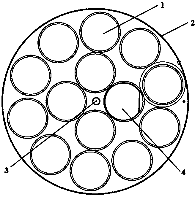
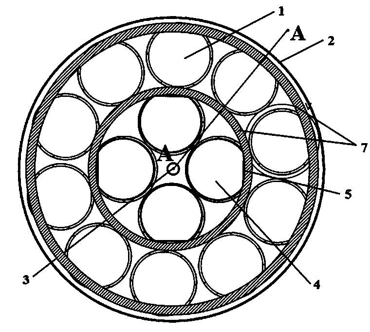
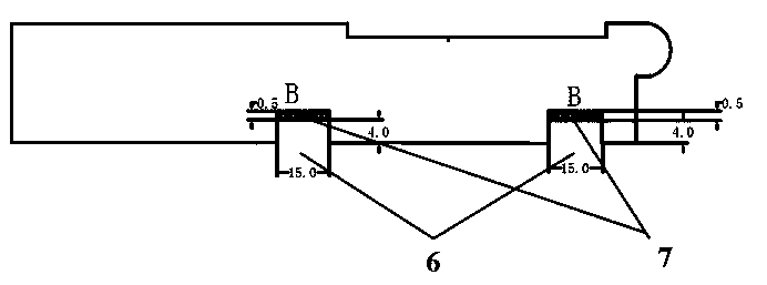
[0038] refer to Figure 2~Figure 3 As shown, the graphite carrier plate that can adjust the local temperature field includes: 14 4-inch (about 100.7mm in diameter) wafer grooves 1 (arranged in two circles, the inner and outer circles, and the circles passing through the center of each wafer groove in the inner and outer rings. Concentric circle relationship), the edge 2 of the graphite carrier plate and the shaft hole 3 arranged in the center of the graphite carrier plate, wherein the wafer groove 1 is arranged above the carrier plate for placing a wafer substrate 4 with a flat edge 5 , and at least two slotted structures 6 are provided on the back of the wafer groove (preferably, the number of slots is consistent with the number of turns of the wafer groove), and the slotted structure is concentric with the graphite carrier plate circle relationship.
[0039] In order to precisely control the temperature at the flat edge position, the slotted structure of the graphite carrie...
Embodiment 2
[0046] refer to Figure 6 As shown, the difference from Embodiment 1 is that Embodiment 1 achieves temperature field balance by increasing the temperature of the local area of the graphite carrier plate, while this embodiment only arranges the slotted structure 6 on the back side of the wafer groove, but does not Filled with thermally conductive material, the slot structure is located below the wafer substrate and close to the center of the graphite carrier plate, so that the temperature field balance can be achieved by reducing the temperature of the local area of the graphite carrier plate, thereby improving the uniformity of the temperature field of the epitaxial wafer On the premise of wavelength uniformity, the manufacturing process is simplified and the manufacturing cost is reduced.
Embodiment 3
[0048] refer to Figure 7 As shown, the difference from Example 2 is that in this embodiment, after the grooved structure is arranged on the back side of the wafer groove, the low thermal conductivity material 8 with a thermal conductivity lower than that of the graphite carrier plate is filled, and the low thermal conductivity material can be selected from ceramics or carbon fibers. Reinforced phenolic resin or polytetrafluoroethylene, carbon fiber reinforced phenolic resin is preferred in this embodiment, and the filling is realized by bonding. This embodiment can effectively overcome the difficulty that the traditional graphite disk cannot control the local temperature field. By reducing the heat conduction in the local area, the uniformity of the temperature field can be precisely controlled, and the wavelength of the 1 / 6 area of the flat side of the 4-inch substrate can be improved. , high defect density at the flat edge position, etc., effectively improving the wavelen...
PUM
 Abstract
Description
Claims
Application Information
 - R&D
- Intellectual Property
- Life Sciences
- Materials
- Tech Scout
- Unparalleled Data Quality
- Higher Quality Content
- 60% Fewer Hallucinations
Browse by: Latest US Patents, China's latest patents, Technical Efficacy Thesaurus, Application Domain, Technology Topic, Popular Technical Reports.
© 2025 PatSnap. All rights reserved.Legal|Privacy policy|Modern Slavery Act Transparency Statement|Sitemap|About US| Contact US: help@patsnap.com


