Method for improving yield of wafer edge
A technology of yield rate and crystal edge, applied in the direction of electrical components, semiconductor/solid-state device manufacturing, circuits, etc.
- Summary
- Abstract
- Description
- Claims
- Application Information
AI Technical Summary
Problems solved by technology
Method used
Image
Examples
Embodiment 1
[0025] S110 , providing a wafer substrate 100 .
[0026] The specific type of substrate to choose can be determined according to product requirements, including substrate material, crystal orientation, doping type, etc., which are not limited here. Silicon substrates are commonly used in this field.
[0027] S120, forming a first photoresist layer by photolithography.
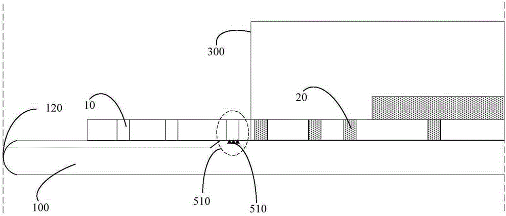
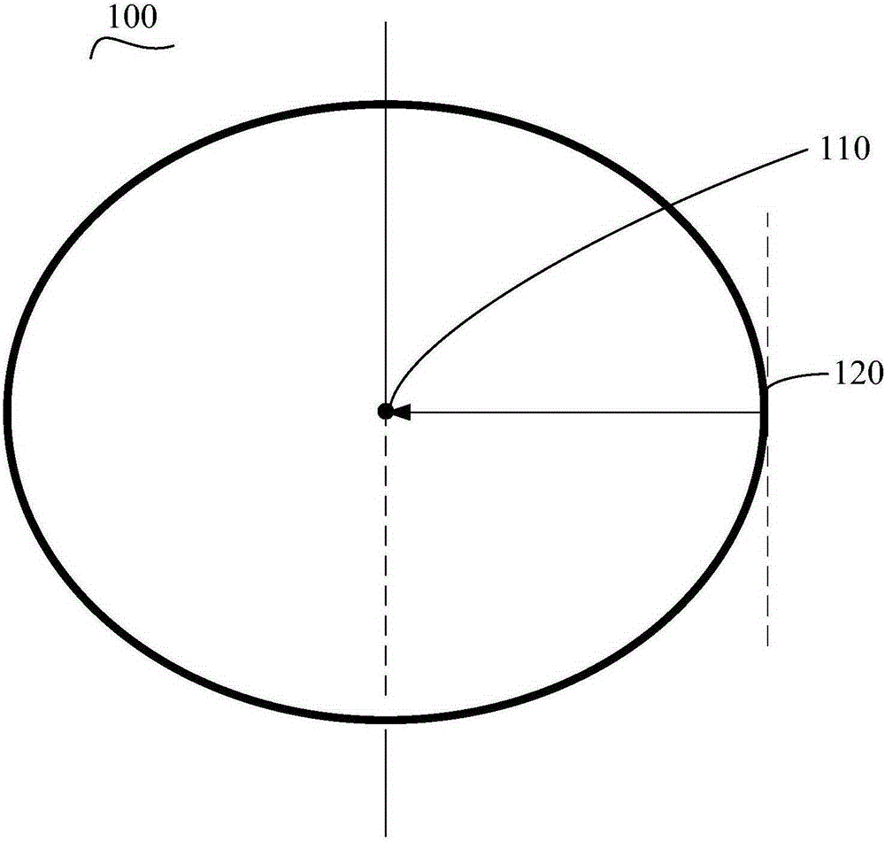
[0028] Please also see Figure 5 , apply glue on the wafer substrate 100 to form the first photoresist layer 210, and perform active area scrubbing (using an organic solvent to remove the photoresist residue at the edge of the wafer) and photolithography. In this embodiment, the wash-off dimension a1 from the edge 120 of the wafer substrate to the axis 110 of the wafer substrate is sufficiently large so that the washed-off area of photoresist extends at least from the edge of the wafer to the subsequent metal deposition The deposition area 300 of the process.
Embodiment 2
[0046] Embodiment 1 is to protect the substrate by forming an oxide layer under the unfilled contact hole 10, and embodiment 2 removes the excess ILD so that no contact hole is formed outside the deposition area 300 to prevent the polishing liquid from passing through the contact hole. 10 The hidden danger of corroding the substrate.
[0047] Therefore, the main difference between Embodiment 2 and Embodiment 1 is that, in step S160, the edge wash size a2 in the direction from the edge 120 of the wafer substrate to the axis 110 of the wafer substrate is reasonably set, so that the area where the photoresist is washed away Extends at least from the edge of the wafer to the deposition area 300 . In this way, in step S170, the excess interlayer dielectric 220 will be etched away, directly avoiding the generation of the contact hole 10 not filled with metal. like Figure 7 shown.
[0048] Same as Embodiment 1, after step S190, a step of forming metal wiring 310 by photolithograp...
PUM
 Abstract
Description
Claims
Application Information
 - R&D
- Intellectual Property
- Life Sciences
- Materials
- Tech Scout
- Unparalleled Data Quality
- Higher Quality Content
- 60% Fewer Hallucinations
Browse by: Latest US Patents, China's latest patents, Technical Efficacy Thesaurus, Application Domain, Technology Topic, Popular Technical Reports.
© 2025 PatSnap. All rights reserved.Legal|Privacy policy|Modern Slavery Act Transparency Statement|Sitemap|About US| Contact US: help@patsnap.com


