A kind of LED display screen and 3D display device thereof
A technology of LED display and LED chip, applied in the direction of identification devices, instruments, electrical components, etc., can solve the problems of increasing driving complexity, serious moiré fringes, strong dazzling feeling, etc., to avoid spot light emission and reduce moire Stripes, simple driving effects
- Summary
- Abstract
- Description
- Claims
- Application Information
AI Technical Summary
Problems solved by technology
Method used
Image
Examples
Embodiment 1
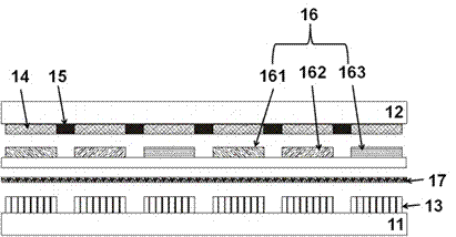
[0052] refer to figure 1 , the present embodiment is a specific scheme when using ultraviolet LED chips, including a first substrate 11; a second substrate 12 opposite to the first substrate; an ultraviolet LED chip array 13 arranged on the first substrate; according to the pixel distribution, set A patterned long-wave pass filter film 14 and a black matrix 15 on the second substrate, the long-wave pass filter film can pass through visible light and reflect ultraviolet light, and the black matrix 15 can reduce or prevent differences between pixels. Color light interference; patterned light conversion material layer 16 arranged according to pixel distribution, said light conversion material layer refers to a material that can absorb ultraviolet light energy and convert this energy into red, green, and blue visible light; short-wave pass filter film 17 , arranged between the patterned light conversion material layer 16 and the ultraviolet LED chip array 13, the short-wave pass f...
Embodiment 2
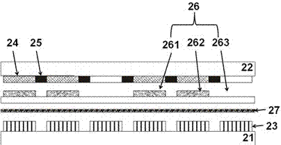
[0063] refer to figure 2 , the present embodiment is a specific scheme when blue LED chips are used, including a first substrate 21; a second substrate 22 opposite to the first substrate; a blue LED chip array 23 arranged on the first substrate; according to pixel distribution, set Patterned long-wave pass filter film 24 and black matrix 25 on the second substrate. The long-wave pass filter film 24 can transmit light with a wavelength longer than blue light and reflect blue light. The black matrix 25 can reduce or prevent each Different color light interference between pixels; patterned light conversion material layer 26 arranged according to pixel distribution, said light conversion material layer refers to a material that can absorb blue light energy and convert the energy into red and green visible light; short-wave pass filter film 27, arranged between the patterned light conversion material layer and the ultraviolet LED chip array, the short-wave pass filter film 27 can ...
Embodiment 3
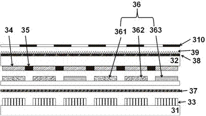
[0074] refer to image 3 In this embodiment, a 3D display device is formed on the basis of the LED display screen in Embodiment 1.
[0075] The LED comprises a first substrate 31; a second substrate 32 opposite to the first substrate; an ultraviolet LED chip array 33 arranged on the first substrate; a patterned long-wave pass filter film 34 arranged on the second substrate according to the pixel distribution And the black matrix 35, the long-wave pass filter film 34 can pass through visible light and reflect ultraviolet light, the black matrix 35 can reduce or prevent the interference of different colors of light between each pixel; the graphic light conversion set according to the pixel distribution Material layer 36, the light conversion material layer refers to materials that can absorb ultraviolet light energy and convert the energy into red, green, and blue visible light; short-wave pass filter film 37 is arranged on the patterned light conversion material layer and the u...
PUM
 Abstract
Description
Claims
Application Information


