Ion implantation monitoring method

An ion implantation and monitoring chip technology, applied in discharge tubes, semiconductor/solid-state device testing/measurement, electrical components, etc., can solve the problems of high risk, low accuracy of monitoring results, affecting calculation results, etc. efficiency, avoiding fluctuations in the intrinsic resistance of semiconductors, and improving accuracy

Active Publication Date: 2014-10-08
BOE TECH GRP CO LTD
View PDF5 Cites 11 Cited by
  • Summary
  • Abstract
  • Description
  • Claims
  • Application Information

AI Technical Summary

Problems solved by technology

However, in this monitoring method, the intrinsic resistance of the silicon wafer substrate fluctuates greatly, which affects the final calculation results. Even if the same implantation conditions and the same annealing conditions are used, the silicon wafer substrates with different intrinsic resistances

Method used


Image

  • Ion implantation monitoring method

Examples


Embodiment Construction

[0020] An embodiment of the present invention provides a monitoring method for ion implantation, which can accurately monitor whether the dose of ion implantation meets the predetermined requirements, and effectively avoids the defect that the monitoring result exceeds the limit caused by the fluctuation of the intrinsic resistance of the substrate in the prior art, and improves The accuracy of monitoring is improved, thereby improving the performance and yield of the device.

[0021] Embodiments of the present invention will be described in detail below in conjunction with the accompanying drawings. The specific embodiments described here are only used to explain the present invention, and are not intended to limit the present invention.

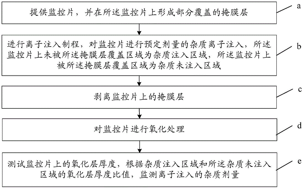
[0022] An embodiment of the present invention provides a method for monitoring ion implantation, such as figure 1 As shown, the method includes:

[0023] a. Provide a monitoring sheet and form a partially covered mask layer on the monitor...


PUM


Abstract

The invention discloses an ion implantation monitoring method and relates to the field of semiconductors. The ion implantation monitoring method can accurately monitor whether the ion implantation amount reaches to the preset requirement, the defect that intrinsic resistance fluctuation of a substrate causes a monitoring result ultra-limit is effectively overcome, the monitoring accuracy is improved, and the device performance and yield are improved. The ion implantation monitoring method comprises the steps of (a) providing a monitoring piece and forming a partially-covered mask layer on the monitoring piece; (b) performing ion implantation processing, and implanting a preset amount of impurity ions into the monitoring piece, wherein a region which is not covered by the mask layer on the monitoring piece is an impurity implantation region, and a region which is covered by the mask layer is an impurity non-implantation region; (c) stripping the mask layer on the monitoring piece; (d) performing oxidation treatment on the monitoring piece; (e) respectively resting the oxide layer thicknesses of the impurity implantation region and the impurity non-implantation region, and monitoring the impurity amount in ion implantation according to oxide layer thickness values of the impurity implantation region and the impurity non-implantation region.

Description

technical field [0001] The invention relates to the fields of display and semiconductor, in particular to a monitoring method for ion implantation. Background technique [0002] Ion implantation is to bombard the surface of the silicon wafer with high-energy ions. At the doping window, the impurity ions are bombarded into the silicon body. In other areas, the impurity ions are shielded by the protective layer on the silicon surface, thereby completing regional selective doping. Ion implantation is a very critical process in the semiconductor manufacturing process. In the field of display and semiconductor manufacturing, different types of semiconductor doped regions can be formed on the semiconductor substrate through ion implantation, which is the basis for forming various device structures. [0003] In the ion implantation process, in order to ensure that the impurity-implanted substrate can achieve predetermined electrical properties, there are strict requirements on the ...

Claims


Application Information

Patent Timeline
IPC IPC(8): H01L21/66
CPCH01L21/67253H01J2237/31703H01J2237/31705H01J2237/31711H01J37/3171H01J37/3005H01J2237/2445
Inventor 田慧
Owner BOE TECH GRP CO LTD
Why Eureka
Try Eureka