
Surface treatment roughening process for electronic copper foils

A technology of surface treatment and electronic copper foil, which is applied in the field of copper foil surface treatment production, can solve the problems that the anti-peel strength has not been significantly improved and the operation is complicated, and achieve the effect of excellent peel strength, high specific surface area and low peak value

Inactive Publication Date: 2014-10-15
SHANDONG JINBAO ELECTRONICS
View PDF10 Cites 8 Cited by
  • Summary
  • Abstract
  • Description
  • Claims
  • Application Information

AI Technical Summary

Problems solved by technology

[0003] The increase of the pressing temperature of the Tg170 sheet will inevitably improve the various properties of the copper foil, especially the peel strength of the copper foil. Fixed current electroplating, the copper foil treated by this method, its anti-peel strength has not been significantly improved, and the operation is more complicated

Method used


Image

  • Surface treatment roughening process for electronic copper foils
  • Surface treatment roughening process for electronic copper foils
  • Surface treatment roughening process for electronic copper foils

Examples


Embodiment 1

[0019] A roughening process for surface treatment of 18 μm electronic copper foil, the steps are as follows:

[0020] (1) Mix and dissolve cathode copper and concentrated sulfuric acid to prepare a roughening solution; wherein, Cu 2+ :20g / L,H 2 SO 4 : 80g / L, the temperature of the roughening solution is 25°C;

[0021] (2) The roughening solution obtained in step (1) is fully mixed and then enters the roughening tank, followed by electroplating with high current density, medium current density and low current density, wherein the high current density is 140A / dm 2 , the plating time is 6s; the medium current density is 70A / dm 2 , the electroplating time is 6s; the low current density is 30A / dm 2 , The electroplating time is 4.5s.

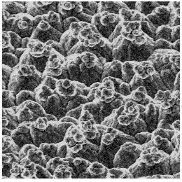
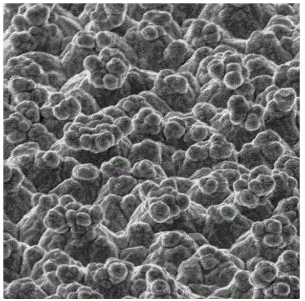
[0022] figure 2 It is the SEM spectrum of the surface roughening effect of the copper foil using Example 1 of the present invention.

[0023] Will figure 1 with figure 2 For comparison, it can be seen that figure 2 The roughened layer of ...

Embodiment 2

[0029] A surface treatment roughening process for electronic copper foil, the steps are as follows:

[0030] (1) Mix and dissolve cathode copper and concentrated sulfuric acid to prepare a roughening solution; wherein, Cu 2+ :40g / L, H 2 SO 4 : 150g / L, the temperature of the roughening solution is 40°C;

[0031] (2) Mix the roughening solution obtained in step (1) fully and then enter the roughening tank, and conduct electroplating through high current density, medium current density and low current density in turn, wherein the high current density is 200A / dm 2 , the plating time is 6s; the medium current density is 90A / dm 2 , the electroplating time is 4.5s; the low current density is 50A / dm 2 , The electroplating time is 6s.

Embodiment 3

[0033] A surface treatment roughening process for electronic copper foil, the steps are as follows:

[0034] (1) Mix and dissolve cathode copper and concentrated sulfuric acid to prepare a roughening solution; wherein, Cu 2+ :30g / L, H 2 SO 4 : 100g / L, the temperature of the roughening solution is 35°C;

[0035] (2) After fully mixing the roughening solution obtained in step (1), enter the roughening tank, and conduct electroplating through high current density, medium current density and low current density in turn, wherein the high current density is 160A / dm 2 , the plating time is 4.5s; the medium current density is 80A / dm 2 , the plating time is 6s; the low current density is 40A / dm 2 , The electroplating time is 6s.


PUM


Abstract

The invention belongs to the technical field of surface treatment production of copper foils, in particular relates to a surface treatment roughening process for electronic copper foils. The surface treatment roughening process comprises the following steps: cathode copper and concentrated sulfuric acid are mixed for dissolving to prepare roughening solution, wherein Cu2+ is 20-40 g / L, H2SO4 is 80-150 g / L, and the temperature of the roughening solution is 25-40 DEG C; and after being fully mixed, the obtained roughening solution is fed in a roughening groove, and is electroplated by high-current density, medium-current density and low-current density in sequence. The roughening process uses one electroplating solution to replace the roughening solution and curing solution with different components, realizes electrolytic copper foils with high specific surface area, low peak value and high binding force through controlling different current densities, and has excellent stripping strength when being applied to plates of Tg 170 and above.

Description

technical field [0001] The invention belongs to the technical field of copper foil surface treatment production, and in particular relates to a surface treatment roughening process of electronic copper foil. Background technique [0002] Electronic copper foil is the basic material for the manufacture of copper clad laminates and printed circuit boards. With the rapid development of the electronics industry, dangerous substances such as lead, mercury, cadmium, hexavalent chromium, polybrominated diphenyl ether or polybrominated biphenyl contained in new electronic and electrical equipment put on the market have brought serious harm to the environment and human health. harm. In recent years, the country has gradually increased its emphasis on environmental protection, prompting the electronics industry to develop in a more environmentally friendly direction, followed by the improvement of technology. Environmentally friendly boards have gradually taken a dominant position, ...

Claims


Application Information

Patent Timeline
Patent Type & Authority Applications(China)
IPC IPC(8): C25D7/06C25D5/00C25D3/38
Inventor 胡旭日王维河王海振薛伟徐好强杨鹏海温世兴姜桂东赵东王天堂尹瑞权赵海燕
Owner SHANDONG JINBAO ELECTRONICS
Learn More