Supercharge Your Innovation With Domain-Expert AI Agents!

L wave band chaotic circuit based on gallium arsenide technology and design method of L wave band chaotic circuit

A chaotic circuit, gallium arsenide technology, applied in the direction of electrical components, digital transmission systems, transmission systems, etc., can solve the problems of changing the working state of the circuit, the basic frequency of chaotic oscillation and the influence of frequency bandwidth, and the inability to generate chaotic signals. Small loss, strong anti-electromagnetic radiation ability, high power effect

Inactive Publication Date: 2014-10-15
RES INST OF SOUTHEAST UNIV IN SUZHOU
View PDF0 Cites 4 Cited by
  • Summary
  • Abstract
  • Description
  • Claims
  • Application Information

AI Technical Summary

Problems solved by technology

However, when the Colpitts circuit works in the high-frequency band, the parasitic capacitance between the electrodes has a significant impact on the basic frequency and bandwidth of the chaotic oscillation, and even changes the working state of the circuit so that it cannot generate chaotic signals.

Method used


Image

  • L wave band chaotic circuit based on gallium arsenide technology and design method of L wave band chaotic circuit
  • L wave band chaotic circuit based on gallium arsenide technology and design method of L wave band chaotic circuit
  • L wave band chaotic circuit based on gallium arsenide technology and design method of L wave band chaotic circuit

Examples


Embodiment Construction

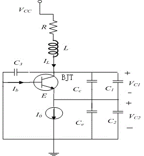
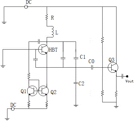
[0025] Such as figure 2 As shown, the L-band chaotic circuit based on gallium arsenide technology disclosed by the present invention considers replacing the silicon BJT with the gallium arsenide technology HBT with less parasitic capacitance as the gain element in the chaotic signal source, so as to reduce the influence of parasitic capacitance on the chaos In addition, due to the sensitivity of the chaotic circuit, a first-stage emitter follower is added to the circuit, and the chaotic signal generated by the circuit is coupled to the emitter follower Q3 through the capacitor C0 to reduce the impact of external perturbation on the circuit state. The impact; the current source adopts the mirror current source composed of Q1 and Q2, which improves the stability of the circuit. All the above devices will be integrated in the chip. The basic structure of the new fully integrated single-chip microwave Colpitts circuit has the characteristics of small circuit loss, low noise, wide...


PUM


Abstract

The invention discloses an L wave band chaotic circuit based on a gallium arsenide technology and a design method of the L wave band chaotic circuit. The L wave band chaotic circuit comprises an HBT, a resonance network and a current source, wherein the HBT is connected through a common base and serves as a booster element in a chaotic signal source, the resonance network is connected with the output end of the HBT and used for generating chaotic signals, and the current source is connected with the emitter of the HBT. The specific design method comprises the steps that a mathematic model of the circuit is established; a circuit state equation with stray capacitance is calculated; state parameters and control parameters are extracted; and model simulation is conducted. According to the L wave band chaotic circuit based on the gallium arsenide technology and the design method of the L wave band chaotic circuit, the gallium arsenide technology HBT with the small stray capacitance is adopted as the booster element in the chaotic signal source, and the influence of the stray capacitance on the working state of the chaotic circuit is reduced; an emitter follower is added in the circuit, and the influence of external perturbation on the state of the circuit is reduced; the current source is formed by a mirror image current source, and the stability of the circuit is improved; a monolithic microwave integrated circuit has the advantages of being small in circuit loss, wide in bandwidth, large in dynamic range, high in additional efficiency and electromagnetic radiation resistance capability and the like.

Description

technical field [0001] The invention relates to an L-band chaotic circuit based on gallium arsenide technology and a design method thereof. Background technique [0002] Due to the characteristics of chaotic signals such as aperiodicity, wide spectrum, noise-like and long-term unpredictability, the application of chaotic signals in military and communication fields has become a major research hotspot. Popular research branches in the military field include: chaotic radar, chaotic control, chaotic countermeasures, chaotic bioelectronics, etc.; applied research in the field of communication involves chaotic secure communication, chaotic carrier digital communication, chaotic sequence frequency hopping spread spectrum and chaotic parameter analysis Multiple access communication, etc., so the study of chaotic circuits is of great significance. At present, the main obstacle is that the frequency of chaotic signals cannot be increased, which limits the application range of chaoti...

Claims


Application Information

Patent Timeline
Patent Type & Authority Applications(China)
IPC IPC(8): H04L9/00
Inventor 蔡士琦孙晓红田婷张晓东
Owner RES INST OF SOUTHEAST UNIV IN SUZHOU
Features
  • R&D
  • Intellectual Property
  • Life Sciences
  • Materials
  • Tech Scout
  • Unparalleled Data Quality
  • Higher Quality Content
  • 60% Fewer Hallucinations
Learn More