Preparation method of self-compensation back-sealing semiconductor substrate

A semiconductor and self-compensating technology, applied in semiconductor/solid-state device manufacturing, electrical components, circuits, etc., can solve the problems of lightly doped epitaxial atmosphere inversion, etc., and achieve the effect of improving quality and efficiency

Active Publication Date: 2014-10-22
BEIJING YANDONG MICROELECTRONICS
View PDF5 Cites 10 Cited by
  • Summary
  • Abstract
  • Description
  • Claims
  • Application Information

AI Technical Summary

Problems solved by technology

[0009] The object of the present invention is to provide a method for growing lightly doped epitaxial layers with opposite conductivity types in batches on heavily doped substrates, so as to solve the inversion of the lightly doped epitaxial atmosphere caused by the self-doping effect and edge effect on the back of the substrate , leading to the problem of growing homoepitaxial layers at the edge of the wafer or the entire substrate

Method used


Image

  • Preparation method of self-compensation back-sealing semiconductor substrate
  • Preparation method of self-compensation back-sealing semiconductor substrate
  • Preparation method of self-compensation back-sealing semiconductor substrate

Examples


Embodiment Construction

[0058] In order to illustrate the present invention more clearly, the present invention will be further described below in conjunction with preferred embodiments and accompanying drawings. Similar parts in the figures are denoted by the same reference numerals. Those skilled in the art should understand that the content specifically described below is illustrative rather than restrictive, and should not limit the protection scope of the present invention.

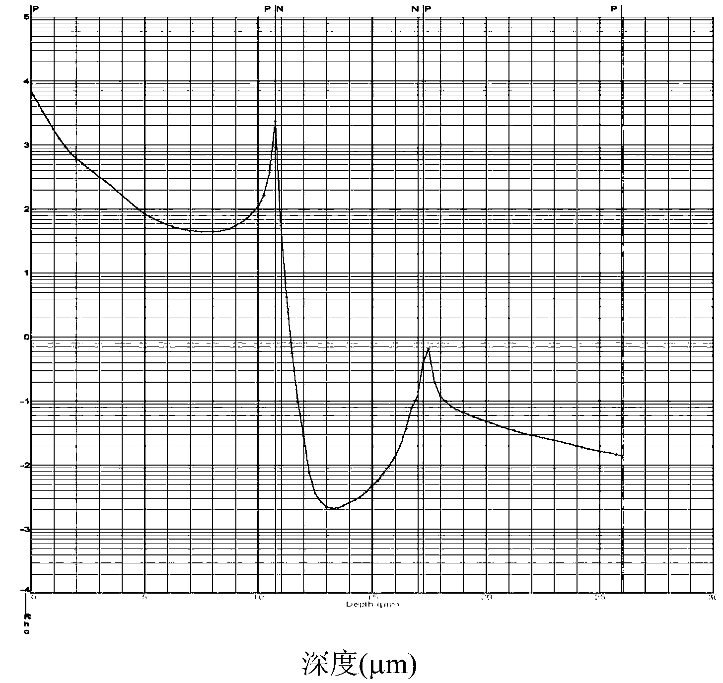
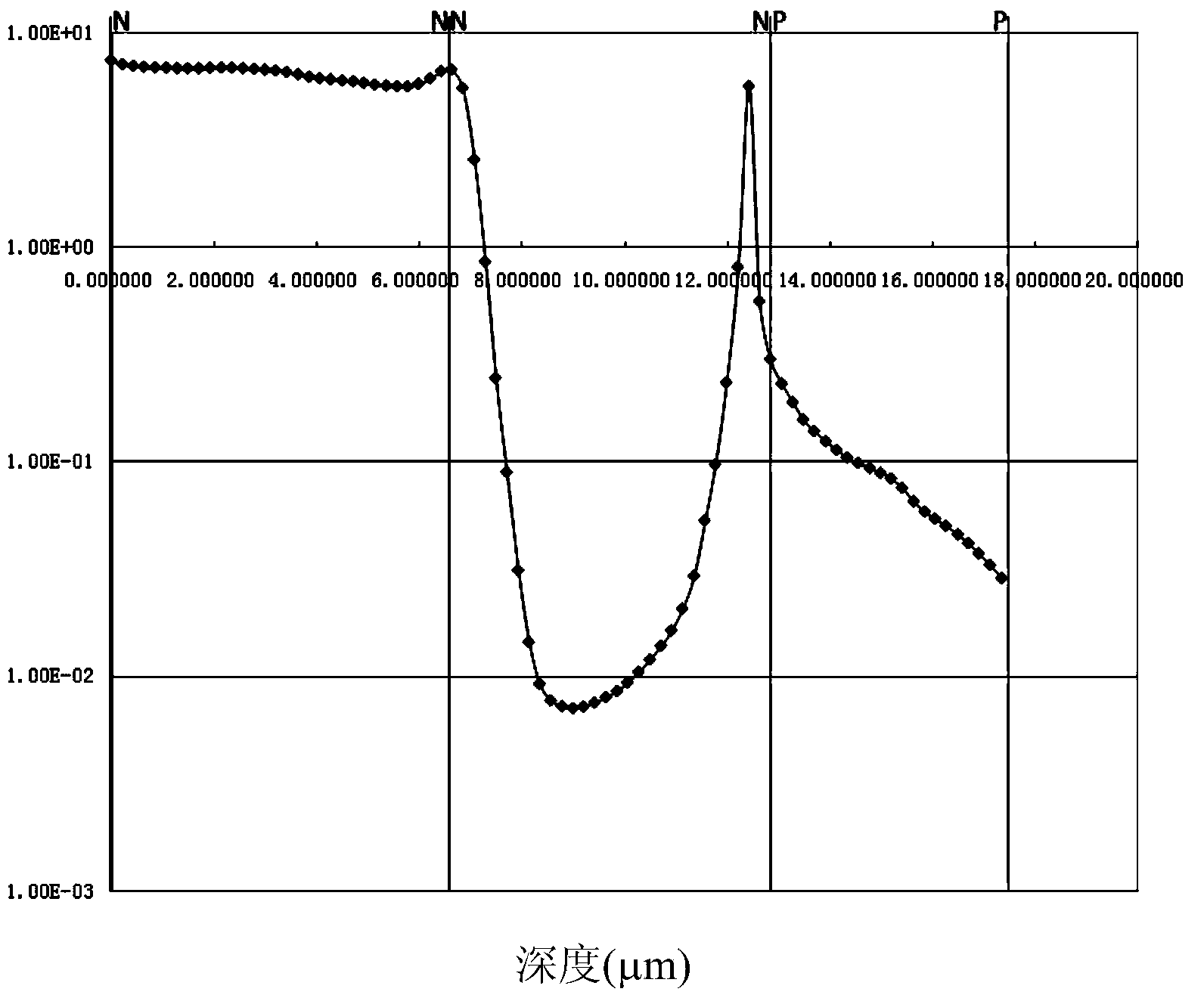
[0059] Figure 3-13 A flow chart of the steps of a method for forming a self-compensating back-sealing substrate and growing an epitaxial layer in a substrate processing stage according to a preferred embodiment of the present invention is shown.

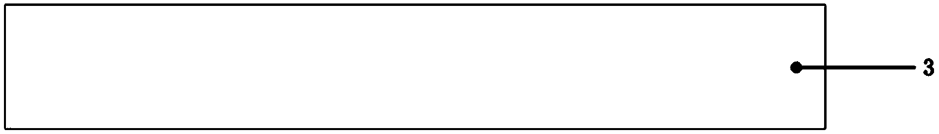
[0060] Provide a heavily doped silicon substrate 3 with a resistivity of the first conductivity type less than 0.01Ω·cm, such as image 3 shown. In this embodiment, the first conductivity type is P-type, and the impurity is boron (B). The resistivity of the P-type doped substr...


PUM

PropertyMeasurementUnit
electrical resistivityaaaaaaaaaa
thicknessaaaaaaaaaa

Abstract

The invention discloses a preparation method of a self-compensation back-sealing semiconductor substrate. The preparation method comprises a technical method of growing an opposite type lightly doped epitaxial layer on a heavily doped substrate. By adopting a mean of producing a self-compensation back sealing layer before the epitaxial growth in the substrate processing stage, the method for growing lightly doped epitaxial layer in opposite conduction type in batches on the heavily doped substrate is provided to solve a problem of same-type epitaxial growth on the inner edge of a chip or the whole chip caused by lightly doped epitaxial atmosphere transoid which is resulted from a backside self-doping effect and an edge effect. With the adoption of the self-compensation back sealing technology, that the epitaxial parameters meet with the product demands still can be guaranteed even full-furnace growth is performed by using a normal-pressure epitaxial furnace.

Description

technical field [0001] The invention relates to the technical field of semiconductor microelectronics, in particular, the invention relates to a method for manufacturing a silicon-based semiconductor device and an integrated circuit. Background technique [0002] With the development of silicon-based semiconductor technology, there are more and more types of semiconductor devices such as discrete devices with specific functions, integrated circuit chips and MOS devices. Various devices have higher and higher requirements on the thickness and concentration of substrates and epitaxial layers. For example, some special devices need to process a lightly doped inversion epitaxial layer on a heavily doped substrate such as a P-type or N-type substrate with a resistivity less than 0.01Ω·cm. As we all know, it is difficult to grow epitaxial layers of the same conductivity type with high resistivity and good uniformity on heavily doped substrates, and it is even more difficult to gr...

Claims


Application Information

Patent Timeline
Patent Type & Authority Applications(China)
IPC IPC(8): H01L21/223
CPCH01L21/2225
Inventor 周源
Owner BEIJING YANDONG MICROELECTRONICS
Why Eureka
Try Eureka