Image real-time correction output method for linear array CCD imaging system based on FPGA

An imaging system and real-time correction technology, applied in image communication, electrical components, etc., can solve problems such as poor correction scheme and output image

Active Publication Date: 2014-10-22
宜宾显微智能科技有限公司
View PDF4 Cites 9 Cited by
  • Summary
  • Abstract
  • Description
  • Claims
  • Application Information

AI Technical Summary

Problems solved by technology

[0005] The purpose of the present invention is to provide a real-time image correction output method of an FPGA-based linear array CCD imaging system,

Method used


Image

  • Image real-time correction output method for linear array CCD imaging system based on FPGA
  • Image real-time correction output method for linear array CCD imaging system based on FPGA
  • Image real-time correction output method for linear array CCD imaging system based on FPGA

Examples


Embodiment

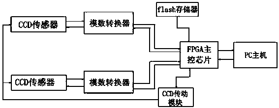
[0047] Such as figure 1 Shown, the present invention is mainly applied to the linear array CCD imaging system aspect based on FPGA, and its hardware aspect, mainly is provided with the FPGA main control chip of algorithm module (being hardware multiplier) and random access memory (being RAM) inside, The analog-to-digital converter whose output end is connected to the input end of the FPGA main control chip, the CCD transmission module connected to the output end of the FPGA main control chip, the flash memory and the PC host that are bidirectionally connected to the FPGA main control chip, and the output terminal It consists of a CCD sensor connected to the input of the analog-to-digital converter and also connected to the CCD transmission module.

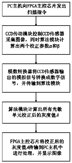
[0048] Based on the above hardware structure, such as figure 2 Shown, the realization process of the present invention is as follows:

[0049] (1) After the system is powered on, the PC host sends scanning instructions to the FP...

example 1

[0067] This example is applied in large-format scanning imaging, such as image 3 , 4 as shown, image 3 is the schematic diagram without correction, Figure 4 It is a schematic diagram after correction. From image 3 It can be seen from the figure that before the correction, the gray value of each pixel is offset from the real value, and the degree of offset is different, so the scanned picture can clearly see that there is a color generation in the distribution, and each The images scanned by each CCD sensor have obvious gaps in the stitching, and some details between pixels affect the observation due to the inconspicuous contrast, which seriously affects the interpretation of the image. After correction, the gray scale is re-stretched to the normal range, the color band is basically removed, the picture quality is significantly improved, and the attributes of the image are more truly reflected, and the details are clearer.

example 2

[0069] Such as Figure 5-9 As shown, in the PCB appearance inspection machine, the picture of the PCB circuit board collected by the CCD sensor is as follows: Figure 5 As shown, the marked 1 and 2 are two identical metal areas. Due to the uneven gray distribution of the image before correction, the gray distribution curves of the same row in areas 1 and 2 will also have large deviations. Figure 6 It is a schematic diagram of gray value distribution in line 10 of area 1 before correction, Figure 7 It is a schematic diagram of the gray value distribution of the 10th line of area 2 before correction. It can be seen that the gray value of the 10th line of area 1 before correction is distributed between 35 and 42, and the average value is 38. The gray value of the 10th line of area 2 is The gray value distribution is between 50 and 65, the average value is 57, and the difference between the two is about 9 gray values. Since the gray distribution of two metals of the same mate...


PUM


Abstract

The invention discloses an image real-time correction output method for a linear array CCD imaging system based on an FPGA. The method includes the following steps: (1) a PC host sends a scanning instruction to an FPGA main control chip; (2) the FPGA main control chip controls CCD sensors to light on and controls a CCD transmission module to control the CCD sensors to acquire images and at the same time, an algorithm module in the FPGA main control chip calculates two correction parameters Alpha and Beta respectively; (3) the CCD sensors acquire image data and transmit the image data to analog-to-digital converters and the analog-to-digital converters convert analog signals into digital signals and transmit the digital signals to the algorithm module in the FPGA main control chip to carry out processing; (4) the algorithm module calculates gray level values corrected by all photosensitive units; (5) the FPGA main control chip transmits the gray level values corrected by the photosensitive units to the PC host for processing so as to form complete images which are then displayed. The image real-time correction output method for the linear array CCD imaging system based on the FPGA is reasonable in design, high in processing speed and high in imaging precision.

Description

technical field [0001] The invention relates to an image output method, in particular to an image real-time correction output method of an FPGA-based linear array CCD imaging system. Background technique [0002] CCD (Charge Coupled Device) image sensor imaging scheme has been widely used in photoelectric detection and image acquisition. Due to the inconsistent responsivity caused by the production process of the CCD photosensitive element, it will cause non-uniform changes in the gray value of the scanned image, which seriously affects the image acquisition quality. Even if the influence of the production process can be ignored, the unevenness of the illumination will also affect the scanned image, so it is very necessary to correct the grayscale of the scanned image. The existing methods that have been proposed are mainly based on the host computer software to achieve correction. For example, some scholars have proposed the analysis and correction of the inhomogeneity of ...

Claims


Application Information

Patent Timeline
IPC IPC(8): H04N1/60H04N1/028
Inventor 陈仕隆张峰杨雷赵泽东吕坤
Owner 宜宾显微智能科技有限公司
Why Eureka
Try Eureka