
NOR-type flash memory unit for lifting common source region and preparation method thereof

A technology of flash memory unit and common source area, which is applied in the direction of electrical components, semiconductor/solid-state device manufacturing, semiconductor devices, etc. It can solve the problems of increased source junction depth, difficulty in normal operation of memory cells, and punch-through, so as to overcome over-etching , It is beneficial to scale down and reduce the effect of short groove effect

Active Publication Date: 2014-10-29
合肥中科微电子创新中心有限公司
View PDF3 Cites 7 Cited by
  • Summary
  • Abstract
  • Description
  • Claims
  • Application Information

AI Technical Summary

Problems solved by technology

On the other hand, in order to use the implantation method to realize the connection of the common source region, it is usually necessary to first remove the insulating layer in the STI. During the etching process, the silicon substrate in the source region is over-etched, and this silicon over-etch further makes Source Junction Depth Increased
With the shortening of the cell trench length, the direct consequence of this asymmetric structure will form a serious punch-through phenomenon, which makes it difficult for the memory cell to work normally.

Method used


Image

  • NOR-type flash memory unit for lifting common source region and preparation method thereof
  • NOR-type flash memory unit for lifting common source region and preparation method thereof
  • NOR-type flash memory unit for lifting common source region and preparation method thereof

Examples


Embodiment Construction

[0037] In order to make the object, technical solution and advantages of the present invention clearer, the present invention will be described in further detail below in conjunction with specific embodiments and with reference to the accompanying drawings.

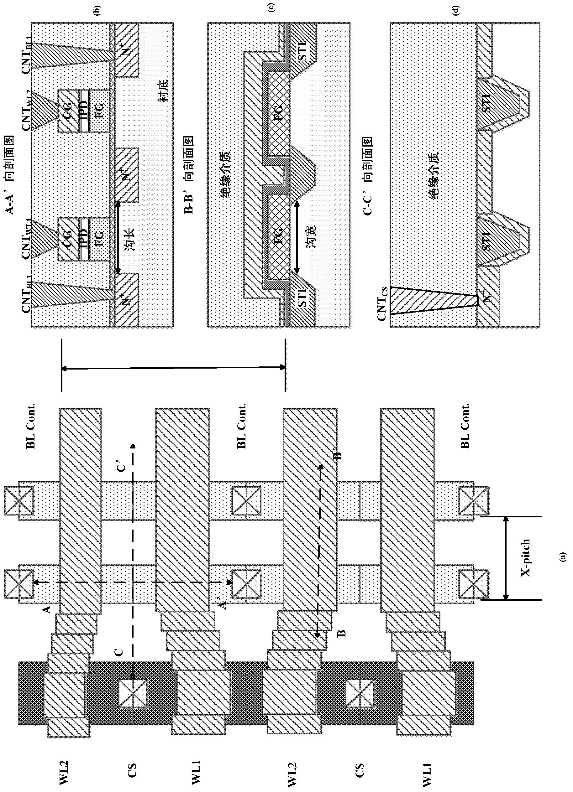
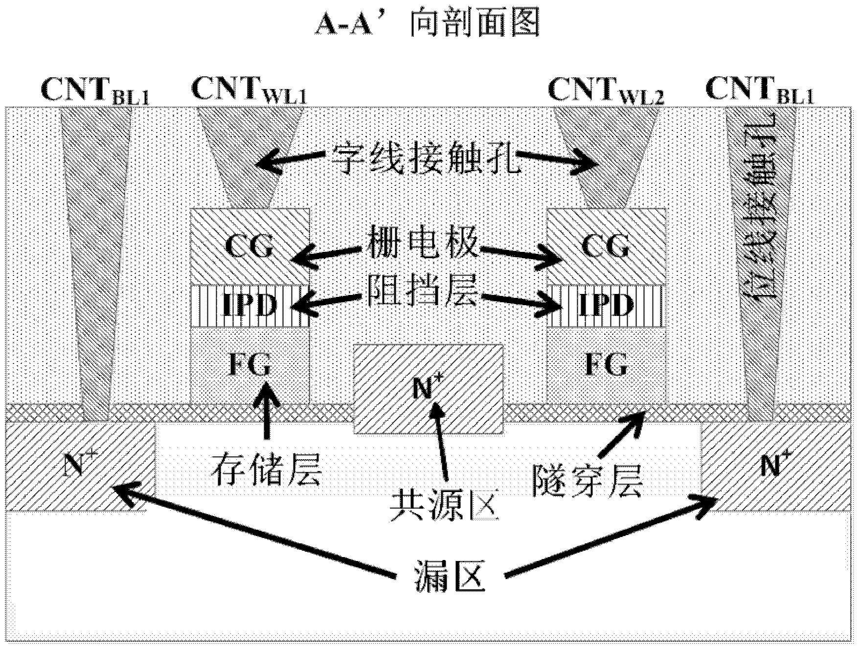
[0038] The key idea of ​​the present invention is to modify the structure of the source area of ​​the flash memory unit. Generally speaking, the shallow trench isolation (STI) region completes the isolation of the active region in the channel width direction of the memory cell, so the source region and the drain region are the same in the channel width direction. The injection of the common source region makes a lateral source deep junction appear. In addition, the etching of the STI region insulating layer in order to realize the connection of the common source region makes silicon over-etching appear in the source region. These two factors are the device trench The main factor that easily causes punch-through when the l...


PUM


Abstract

The invention discloses an NOR-type flash memory unit for lifting a common source region and a preparation method thereof. The flash memory unit comprises a substrate; common source and drain regions formed below the surface of the substrate through injection; a channel region formed on the surface of the substrate between the common source and drain regions; a tunneling layer formed over the channel region; a storage layer formed over the tunneling layer; a barrier layer formed over the storage layer; and a gating electrode formed over the barrier layer. In the forming process of the common source region, an epitaxial process is first used for lifting the common source region, and then low resistance connection is formed between below the shallow slot isolation region and the common source region through ion injection for below a shallow slot isolation region and the common source region of the flash memory unit. Through the introduction of the epitaxial process, the shallow slot isolation region expands along an active region in a channel width direction along while the common source region is lifted, punch-through effects are effectively simulated in the size reduction process of a conventional NOR-type flash memory device, and the NOR-type device is further scaled down in a channel length direction.

Description

technical field [0001] The invention belongs to the technical field of microelectronic devices and memories, and in particular relates to a NOR type flash memory unit with a raised common source region and a preparation method thereof. Background technique [0002] Semiconductor storage technology is one of the key technologies in the field of microelectronics technology. As information technology shifts from network and computing to storage as the core, the research on storage technology has become an important direction of information technology research. As an important product type, flash memory has developed rapidly in recent years due to the expansion of markets such as multimedia and smart phones. Flash memory mainly includes NOR flash memory and NAND flash memory. NOR flash memory is usually used for code storage because of its high-speed characteristics, and it is more common in mobile phones and communication chips. [0003] Conventional NOR-type flash memory chi...

Claims


Application Information

Patent Timeline
IPC IPC(8): H01L27/115H01L29/08H01L21/8247H01L21/762
Inventor 霍宗亮刘明
Owner 合肥中科微电子创新中心有限公司
Learn More