LDMOS device based on high K material
A technology of devices and drift regions, which is applied in the field of electronics and can solve problems such as large leakage currents
- Summary
- Abstract
- Description
- Claims
- Application Information
AI Technical Summary
Problems solved by technology
Method used
Image
Examples
Embodiment Construction
[0022] Specific embodiments of the present invention will be further described in detail below.
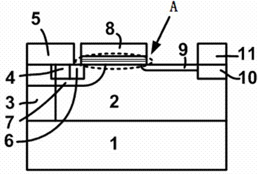
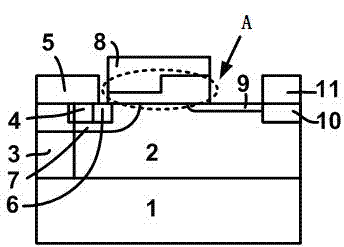
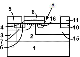
[0023] Such as figure 1 As shown, taking N-type LDMOS as an example, a kind of LDMOS device based on a high-K material in the first preferred embodiment of the present invention includes a highly doped substrate 1, and the resistivity of the substrate 1 is usually 0.005-0.05Ω ·cm 0.005|0.05Ω|cm, there is an epitaxial layer 2 on the highly doped substrate 1, and its resistivity is usually 10-100Ω·cm. The source 6 and the drain 10 are composed of heavily doped N-type, and their doping concentration is usually between Above, the metal wire 5 and the metal wire 11 are metal wires used to connect the source and the drain respectively. The N-type doped drift region 9 is used to improve the breakdown voltage of the LDMOS device. P-type heavy doping 4 is used to provide a fixed potential for the P-type channel to prevent parasitic Bipolar conduction. P-Body7 is used to form the chann...
PUM
 Abstract
Description
Claims
Application Information


