
A double-bit junction-free flash memory and its programming, erasing and reading methods

A technology of flash memory and flash memory, which is applied in static memory, read-only memory, information storage, etc., can solve problems such as high reliability requirements, slow reading, writing, and erasing speed, and complex circuit structure, etc. Small short trench effect, reduce process steps and cost, and solve the effect of complex circuit structure

Active Publication Date: 2018-06-29
SHANGHAI HUALI MICROELECTRONICS CORP
View PDF6 Cites 0 Cited by
  • Summary
  • Abstract
  • Description
  • Claims
  • Application Information

AI Technical Summary

Problems solved by technology

[0012] The purpose of the present invention is to overcome the above-mentioned defects existing in the prior art, and provide a double-bit junction-free flash memory and its programming, erasing and reading methods, which can solve the complex circuit structure of the traditional floating gate multi-bit storage technology. Defects with slow reading, writing, and erasing speeds and high reliability requirements

Method used


Image

  • A double-bit junction-free flash memory and its programming, erasing and reading methods
  • A double-bit junction-free flash memory and its programming, erasing and reading methods
  • A double-bit junction-free flash memory and its programming, erasing and reading methods

Examples


Embodiment Construction

[0041] The specific embodiment of the present invention will be further described in detail below in conjunction with the accompanying drawings.

[0042] It should be noted that, in the following specific embodiments, when describing the embodiments of the present invention in detail, in order to clearly show the structure of the present invention for the convenience of description, the structures in the drawings are not drawn according to the general scale, and are drawn Partial magnification, deformation and simplification are included, therefore, it should be avoided to be interpreted as a limitation of the present invention.

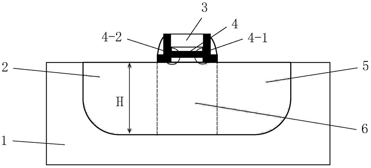
[0043] In the following specific embodiments of the present invention, please refer to figure 1 , figure 1 It is a structural schematic diagram of a dual-bit junction-free flash memory in a preferred embodiment of the present invention. Such as figure 1 As shown, a dual-bit junctionless flash memory memory of the present invention includes: a P-ty...


PUM


Abstract

The invention discloses a double-bit junction-free flash memory, which is a SONOS flash memory using a junction-free transistor structure, and its substrate has a source terminal, a drain terminal and a channel region uniformly and heavily doped with N-type impurities without using PN Junction, whose silicon nitride layer includes two storage bits for storing charge, whose heavily doped region has a thickness that enables the SONOS flash memory to completely deplete the region of electrons when it is turned off; its programming utilizes band tunneling hot space The method of hole injection is used for erasing, and the channel FN tunneling erasure mechanism is used for erasing, and the reverse reading method is used for reading, which can solve the complex circuit structure existing in traditional floating gate multi-bit storage technology. In addition to the defects of slower speed and higher reliability requirements.

Description

technical field [0001] The present invention relates to the technical field of semiconductors, more specifically, to a dual-bit junctionless flash memory and programming, erasing and reading methods thereof. Background technique [0002] As the distance between the PN junctions of modern CMOS devices has reached the sub-50nm stage, extremely high doping concentration gradients are necessary, which greatly increases the difficulty of process manufacturing. When the channel length of the device is less than 50nm, the ultra-shallow junction technology is very effective in suppressing the short-channel effect, but it is difficult to control the depth and profile of the PN junction. Moreover, due to the high cost of thermal annealing, the formation of ultra-shallow junctions is a bottleneck for future 3D multilayer stacked device processes. [0003] SONOS (Silicon-Oxide-Nitride-Oxide-Silicon, Silicon-Oxide-Nitride-Oxide-Silicon) is a non-volatile memory that is closely related t...

Claims


Application Information

Patent Timeline
Patent Type & Authority Patents(China)
IPC IPC(8): H01L27/11568H01L29/423G11C16/10G11C16/14H10B43/30H10B69/00
Inventor 顾经纶
Owner SHANGHAI HUALI MICROELECTRONICS CORP
Learn More