Perovskite solar battery and preparation method thereof
A technology of solar cells and perovskite, applied in the field of solar cells, can solve the problems of high cost of preparation and application of perovskite solar cells, and achieve the effects of suppressing the carrier recombination effect, simplifying the manufacturing process and reducing the production cost.
- Summary
- Abstract
- Description
- Claims
- Application Information
AI Technical Summary
Problems solved by technology
Method used
Image

Examples
Embodiment 1
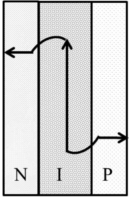
[0043] Use CH 3 NH 3 PB 3 As the perovskite material in perovskite solar cells, mesoporous conductive carbon is used as the counter electrode layer. The specific preparation steps are as follows:
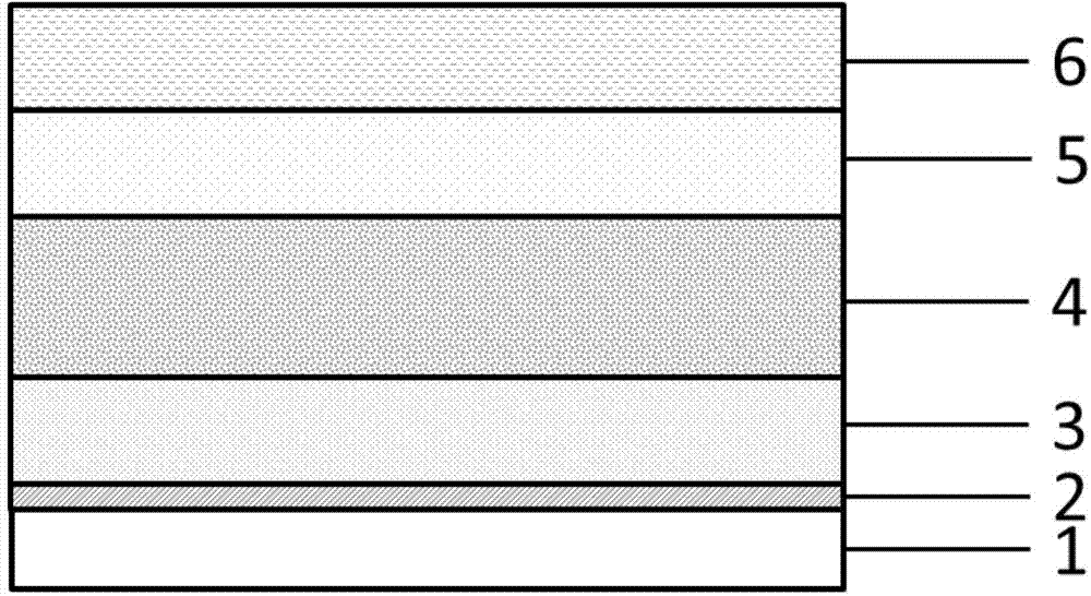
[0044] (1) Deposit a layer of dense TiO on the cleaned transparent FTO conductive glass substrate by spray pyrolysis 2 layer, with a thickness of about 50nm, and heat treatment at 450°C for 40min to form a dense layer;
[0045] (2) TiO with a particle size of 20nm 2 The slurry was uniformly coated on dense TiO by screen printing 2 layer, and dried at 125°C for 10 minutes to form an n-type semiconductor layer with a thickness of 300nm;
[0046] (3) ZrO with a particle size of 30nm 2 The slurry was also uniformly coated on TiO by screen printing. 2 layer, and dried at 125°C for 15 minutes to form an insulating layer with a thickness of 400nm;
[0047] (4) Evenly coat the NiO slurry with a particle size of 20nm on the ZrO by screen printing. 2 layer, and dried at 125°C for 15 ...
Embodiment 2
[0053] Use CH 3 NH 3 PB 3 As the perovskite material in perovskite solar cells, metal Au is used as the counter electrode layer, and the specific preparation steps are as follows:
[0054] (1) Deposit a layer of dense TiO on the cleaned transparent FTO conductive glass substrate by spray pyrolysis 2 layer, with a thickness of about 50nm, and heat treatment at 450°C for 40min to form a dense layer;
[0055] (2) TiO with a particle size of 20nm 2 The slurry was uniformly coated on dense TiO by screen printing 2 layer, and dried at 125°C for 10 minutes to form an n-type semiconductor layer with a thickness of 100nm;
[0056] (3) ZrO with a particle size of 30nm 2 The slurry was also uniformly coated on TiO by screen printing. 2 layer, and dried at 125°C for 15 minutes to form an insulating layer with a thickness of 200nm;
[0057] (4) Evenly coat the NiO slurry with a particle size of 20nm on the ZrO by screen printing. 2 layer, and dried at 125°C for 15 minutes to form ...
Embodiment 3
[0063] Use CH 3 NH 3 PB 3As the perovskite material in perovskite solar cells, mesoporous conductive carbon is used as the counter electrode layer. The specific preparation steps are as follows:
[0064] (1) Deposit a dense NiO layer on the cleaned transparent FTO conductive glass substrate by spray pyrolysis, with a thickness of about 80nm, and heat-treat at 500°C for 30min to form a dense layer;
[0065] (2) Evenly coat the NiO slurry with a particle size of 20nm on the dense NiO layer by screen printing method, and dry at 125°C for 10min to form a p-type semiconductor layer with a thickness of 300nm;
[0066] (3) ZrO with a particle size of 30nm 2 The slurry is also evenly coated on the NiO layer by screen printing, and dried at 125°C for 15 minutes to form an insulating layer with a thickness of 400nm;
[0067] (4) TiO with a particle size of 20nm 2 The paste was uniformly coated on ZrO by screen printing 2 layer, and dried at 125°C for 15 minutes to form an n-type s...
PUM
 Abstract
Description
Claims
Application Information
 - R&D
- Intellectual Property
- Life Sciences
- Materials
- Tech Scout
- Unparalleled Data Quality
- Higher Quality Content
- 60% Fewer Hallucinations
Browse by: Latest US Patents, China's latest patents, Technical Efficacy Thesaurus, Application Domain, Technology Topic, Popular Technical Reports.
© 2025 PatSnap. All rights reserved.Legal|Privacy policy|Modern Slavery Act Transparency Statement|Sitemap|About US| Contact US: help@patsnap.com