Multi-wavelength laminated fluorescence data memory, device manufacturing method of multi-wavelength laminated fluorescence data memory and reading method of multi-wavelength laminated fluorescence data memory

A technology of data memory and data access device, which is applied in the field of optical information storage, can solve problems such as technical difficulties, and achieve the effects of light excitation, fast and stable reading, and good stability

Active Publication Date: 2014-11-05
NANJING UNIV OF POSTS & TELECOMM
View PDF6 Cites 4 Cited by
  • Summary
  • Abstract
  • Description
  • Claims
  • Application Information

AI Technical Summary

Problems solved by technology

[0006] Therefore, for multi-layer memory, it is not only required to be able to store sufficient information, to respond quickly, but also to require a high signal-to-noise ratio, which is difficult to achieve with existing technologies.

Method used


Image

  • Multi-wavelength laminated fluorescence data memory, device manufacturing method of multi-wavelength laminated fluorescence data memory and reading method of multi-wavelength laminated fluorescence data memory
  • Multi-wavelength laminated fluorescence data memory, device manufacturing method of multi-wavelength laminated fluorescence data memory and reading method of multi-wavelength laminated fluorescence data memory
  • Multi-wavelength laminated fluorescence data memory, device manufacturing method of multi-wavelength laminated fluorescence data memory and reading method of multi-wavelength laminated fluorescence data memory

Examples


Embodiment Construction

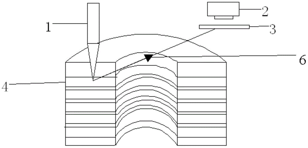
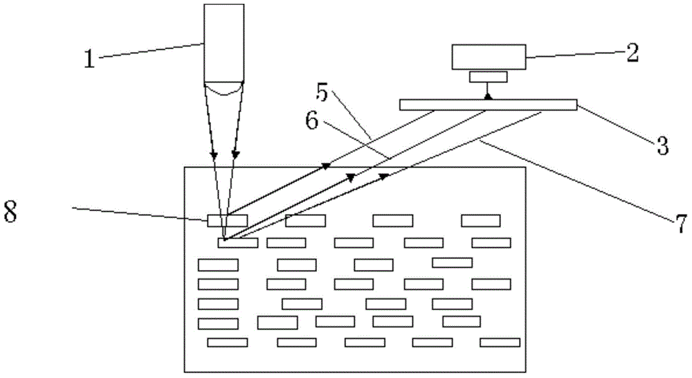
[0043] Attached below figure 1 and figure 2 The technical scheme of the present invention is described in detail:

[0044] The idea of ​​the present invention is to use incident laser light to irradiate the information layer to be read in the fluorescent memory, and generate a fluorescent signal when the fluorescent medium in the groove of the information bit on the information layer absorbs energy. The fluorescent signal, because it is different from other wavelengths, finally uses a filter in the CCD detector to filter out wavelengths other than the fluorescent wavelength excited by the information layer to be read, so as to ensure that the CCD receives only the fluorescent signal from the information layer to be read.

[0045] The structure of the fluorescent memory device of the present invention is as follows figure 1As shown, it includes an incident laser 1, a CCD detector 2, a multi-wavelength filter 3, and an information layer 4 coated with a fluorescent fluorescent...


PUM


Abstract

The invention discloses a multi-wavelength laminated fluorescence data memory, a device manufacturing method of the multi-wavelength laminated fluorescence data memory and a reading method of the multi-wavelength laminated fluorescence data memory, and belongs to an optical information storage technology. The multi-wavelength laminated fluorescence data memory, the device manufacturing method and the reading method provided by the invention have a thought that incident laser is used and is irradiated onto an information layer to be read of a fluorescence memory; fluorescence signals are generated when fluorescence media in a groove of an information bit of the information layer absorbs energy; the wavelength of the fluorescence signals is different from that of others, so that a CCD (Charge Coupled Device) detector uses one filter plate to filter out the signals with the wavelength beyond the wavelength of the fluorescence excited by the information layer to be read, and a CCD is enabled to only receive the fluorescence signals of the information layer to be read; and after the reading completion of one layer of information, a computer is used for controlling a filter to be switched to the filter plate corresponding to the information layer to be read. The condition that the fluorescence signals received by the CCD only contain the signals of the information layer to be read is ensured, so that the goal of layer selection is achieved.

Description

[0001] technical field [0002] The invention belongs to the technology of optical information storage, and in particular relates to the production of fluorescent materials and a memory reading method. [0003] Background technique [0004] Optical data storage technologies such as CD and DVD discs have been widely used in audio-visual and computer data storage fields. Optical information storage technology is a technology that irradiates the medium with laser light, causes physical and chemical changes in the medium through the interaction between the laser and the medium, and stores information. In order to meet the needs of the development of computer technology, the data storage capacity of storage devices is increasing at a rate of 60% every year. At present, people are trying to find ways to further increase the storage capacity of the memory. At this stage, the method of increasing the capacity of storage devices is to increase the magnetic and The storage density ...

Claims


Application Information

Patent Timeline
Patent Type & Authority Applications(China)
IPC IPC(8): G11B7/26G11B7/135
Inventor 黄维杨涛李元义李奥周馨慧仪明东
Owner NANJING UNIV OF POSTS & TELECOMM
Why Eureka
Try Eureka