STT-MRAM (Spin-transfer torque magnetic random access memory) memory cell

A technology for memory cells and MOS devices, applied in the field of transistors, can solve problems such as wasted area, achieve large applicability, reduce device size, and improve read and write stability.

Inactive Publication Date: 2014-11-05
SHANGHAI INTEGRATED CIRCUIT RES & DEV CENT +1
View PDF4 Cites 7 Cited by
  • Summary
  • Abstract
  • Description
  • Claims
  • Application Information

AI Technical Summary

Problems solved by technology

[0008] The 2T-1R method of STT MRAM disclosed in the above literature improves the stability of reading and writing, but requires two MOS transistors in STT MRAM, which is a waste of area

Method used


Image

  • STT-MRAM (Spin-transfer torque magnetic random access memory) memory cell
  • STT-MRAM (Spin-transfer torque magnetic random access memory) memory cell
  • STT-MRAM (Spin-transfer torque magnetic random access memory) memory cell

Examples


Embodiment 1

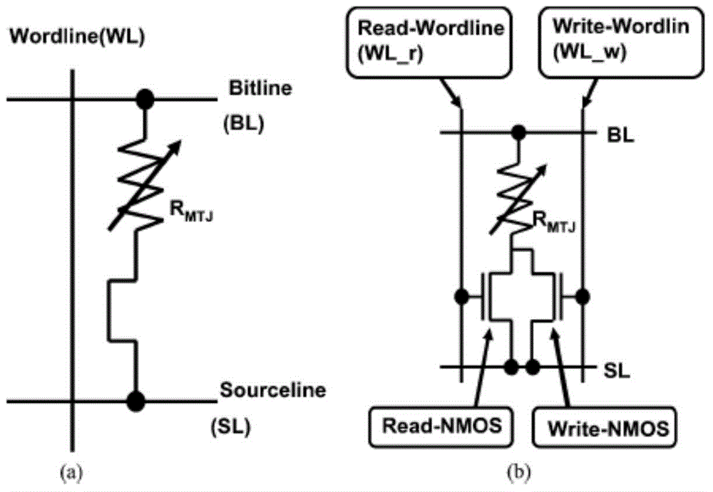
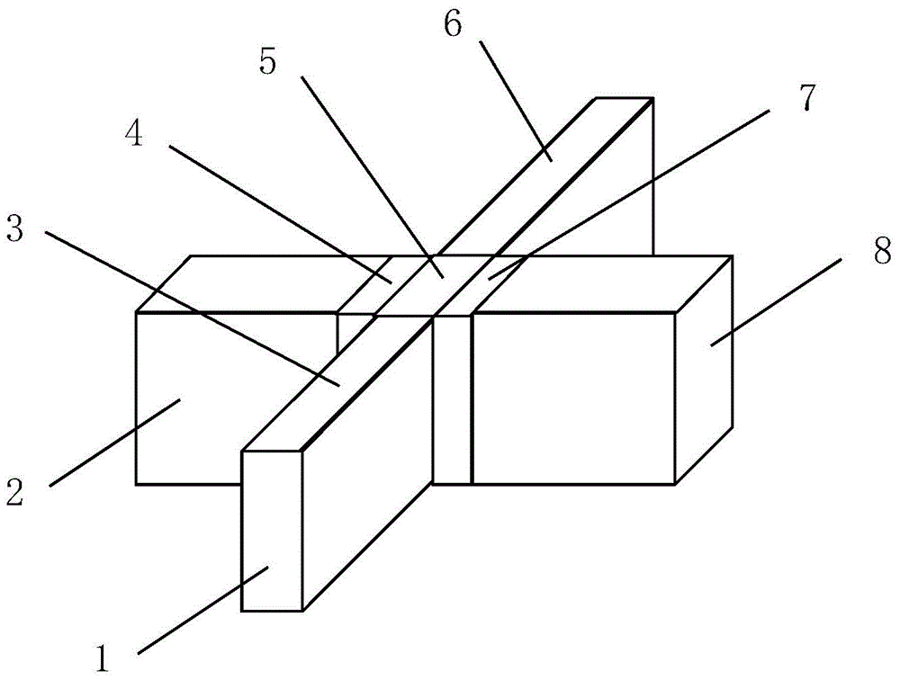
[0031] In this example, see figure 2 , figure 1 It is a structural schematic diagram of a FinFET device of an STT-MRAM storage unit in the present invention. The STT-MRAM storage unit of the present invention includes a magnetic tunnel junction and a selection transistor, and the transistor is a Fin Field Effect Transistor (FinFET). As shown in the figure, the figure is a schematic structural diagram of a FinFET device. The FinFET in the figure includes a silicon fin (Fin) 1 structure formed on a substrate and two gates 2 and 8 independent of each other. Both ends of Fin1 have a source region 3 and a drain region 6, and two gates 2 and 8 are located on both sides of Fin1, specifically on both sides of the channel region between the source region 3 and the drain region 6 of Fin1. Wherein, the gate 2 and the source region 3 and the drain region 6 of Fin1 constitute a MOS device; the gate 8 and the source region 3 and drain region 6 of Fin1 constitute another MOS device. The...

Embodiment 2

[0049] In this example, see Figure 4 , Figure 4It is another structural schematic diagram of a FinFET device of an STT-MRAM storage unit in the present invention. In Embodiment 1, the FinFET device uses one Fin as the driving device in the STT-MRAM unit. The present invention can also cover the situation when there are multiple Fins, that is, the FinFET device can be controlled according to the driving needs of the MTJ. Configure multiple Fins. For example, if the MTJ needs to be driven at about 150 μA, the above-mentioned single Fin device is not applicable, and a double Fin structure is required to provide a driving current of 150 μA. The read current can be adjusted as needed. Generally, a small read current will improve stability, but too small will also affect the read speed. This patent provides a more flexible option, for example, for double Fin situations, such as Figure 4 As shown, the FinFET device has a double Fin1-1 and 1-2 structure, the source and drain re...

Embodiment 3

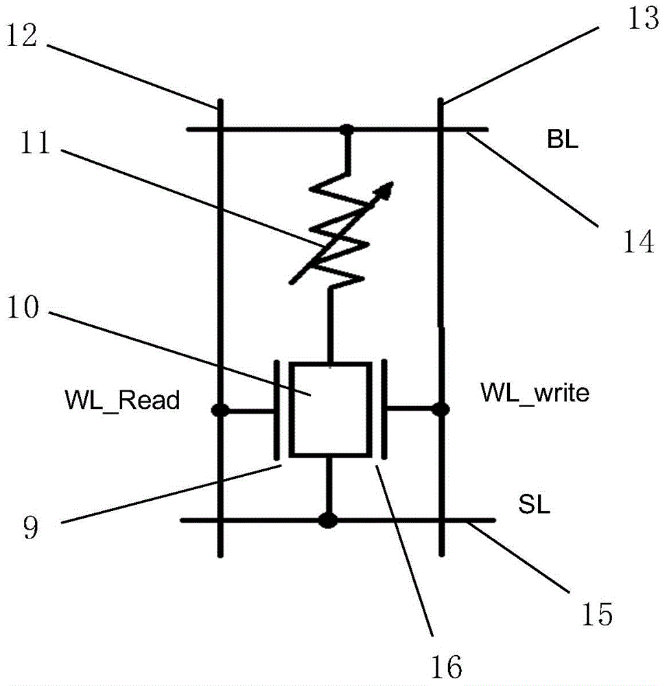
[0051] In this example, Figure 4 The FinFET device in the device can also be used in the following circuit connection mode (the schematic diagram of the circuit structure is omitted): the gate 8-1 and 2-2 connected together are connected to the read word line end of the STT-MRAM memory cell; The poles 2-1 and 8-2 are interconnected through metal, and are connected to the writing word line terminal of the STT-MRAM storage unit. The drain ends of the two Fin1-1 and 1-2 are connected in parallel to one end of the magnetic tunnel junction, and the source end is connected in parallel to the ground wire of the STT-MRAM memory cell; the other end of the magnetic tunnel junction is connected to the bit line of the STT-MRAM memory cell . In this case, the reading speed of the cell will be faster. In actual design, it can be configured in the manner of Embodiment 2 or Embodiment 3 according to application requirements.


PUM


Abstract

The invention discloses a STT-MRAM (spin-transfer torque magnetic random access memory) storage cell; a transistor of the STT-MRAM storage unit is designed into a FinFET (Fin Field-Effect Transistor) form with independent double gates, two MOS (metal oxide semiconductor) devices are formed respectively by two gate electrodes on both sides of the Fin and a Fin source, and a drain region, the two MOS devices share the source and the drain region, and the two gate electrodes are mutually back gates, and can respectively control Fin to open or close a conductive channel; by use of the gate-controlled features of a FinFET device with the independent double gates, the two MOS devices are formed in one FinFET device to achieve a small read current and a larger write current required by the STT-MRAM storage cell, the STTMRAM read-write stability can be effectively improved, and the size of the device can be further reduced under the same drive current conditions.

Description

technical field [0001] The present invention relates to a storage unit of STT-MRAM (Spin Transfer Torque-Magnetic Random Access Memory, spin transfer torque magnetic storage), more particularly, relates to a transistor of a storage unit of STT-MRAM. Background technique [0002] The second-generation magnetic memory (Magnetic Random Access Memory, MRAM) is the spin transfer torque magnetic memory (Spin Transfer Torque-Magnetic Random Access Memory, STT-MRAM) is the most likely to replace DRAM (Dynamic Random Access Memory, dynamic random access memory) and SRAM (Static Random Access Memory, static random access memory) advanced storage technology. The read stability and write stability of STT-MRAM are key performance indicators that determine whether STT-MRAM can be mass-produced. [0003] The read and write functions of STT-MRAM are controlled by the storage unit of STT-MRAM. At present, a typical STT-MRAM memory cell is composed of a magnetic tunnel junction (Magnetic Tu...

Claims


Application Information

Patent Timeline
Patent Type & Authority Applications(China)
IPC IPC(8): G11C11/16H01L43/00
CPCG11C11/1659
Inventor 胡少坚王全陈寿面任铮郭奥
Owner SHANGHAI INTEGRATED CIRCUIT RES & DEV CENT
Why Eureka
Try Eureka