Semiconductor device, transparent metal mesh electrode, and preparation method of transparent metal mesh electrode

A technology of mesh electrodes and manufacturing methods, which is applied to semiconductor devices, circuits, electrical components, etc., and can solve the problems of unsatisfactory optical performance of nanometer metal grid wires, etc.

Inactive Publication Date: 2014-11-05
INST OF SEMICONDUCTORS - CHINESE ACAD OF SCI
View PDF3 Cites 10 Cited by
  • Summary
  • Abstract
  • Description
  • Claims
  • Application Information

AI Technical Summary

Problems solved by technology

Its electrical conductivity is much better than that of ITO film, but at the same time, the width of th

Method used


Image

  • Semiconductor device, transparent metal mesh electrode, and preparation method of transparent metal mesh electrode
  • Semiconductor device, transparent metal mesh electrode, and preparation method of transparent metal mesh electrode
  • Semiconductor device, transparent metal mesh electrode, and preparation method of transparent metal mesh electrode

Examples


example 1

[0033] Example 1, using a transparent metal mesh electrode instead of the traditional annealed ITO transparent electrode layer to form an ohmic contact in a front-mount LED structure, including steps:

[0034] Step 1: Clean the LED epitaxial wafer;

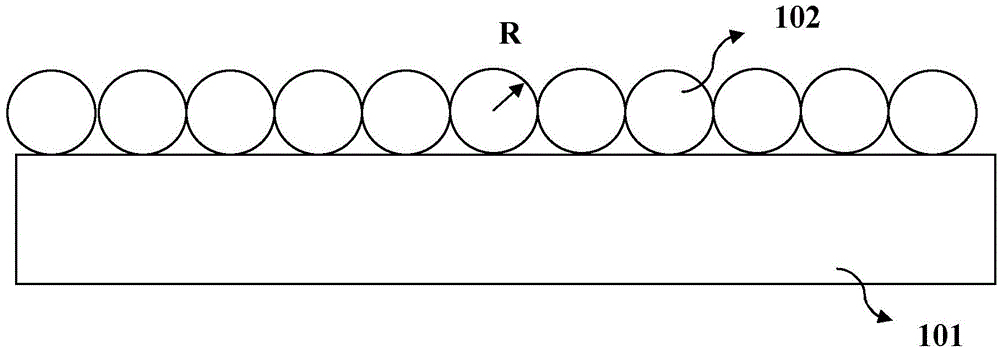
[0035] Step 2: Lay PS balls on the LED epitaxial wafer p-GaN structure by pulling method;

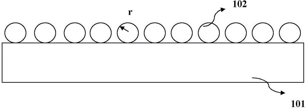
[0036] Step 3: Shrunk the ball using plasma etching method;

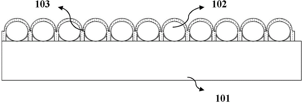
[0037] Step 4: Evaporate 10nm thick metal Pt;

[0038] Step 5: Clean and remove the PS balls to obtain a transparent metal Pt mesh electrode to form an ohmic contact with p-GaN;

[0039] Step 6: Carry out follow-up processes such as photolithography mesa, metal mesh electrode corrosion, and ICP mesa etching.

example 2

[0040] Example 2, see Figure 1 to Figure 5 , including the following steps:

[0041] Step 1: Select a cleaned sapphire substrate, and use the pulling method to lay a single layer of PS balls with a diameter of about 900nm on the surface;

[0042] Step 2: Use plasma etching method to shrink the ball, and reduce the diameter of the PS ball to about 870nm;

[0043] Step 3: using a vacuum evaporation method to evaporate a 30nm thick Ni metal layer on the substrate after shrinking the ball;

[0044] Step 4: cleaning the substrate after metal evaporation, removing the PS ball and the metal film covering it, and obtaining a transparent metal Ni mesh film electrode layer with a slight metallic luster.


PUM


Abstract

The invention discloses a transparent electrode and a preparation method thereof. A transparent metal mesh electrode replaces the traditional annealing ITO (Indium Tin Oxide) transparent electrode layer to form ohmic contact in a positive LED (Light Emitting Diode) structure. According to the transparent electrode and the preparation method, a periodic structure is laid as a mask laying metal electrode by a self-assembly method, a transparent function of the electrode is achieved by holes of metal meshes, and the light transmissivity of the electrode can be controlled by controlling an area ratio of holes of a metal film.

Description

technical field [0001] The invention belongs to the technical field of microelectronics and semiconductors, and relates to a semiconductor device, a transparent metal mesh electrode and a manufacturing method thereof. Background technique [0002] Transparent electrodes are widely used in displays, especially touch displays, LEDs, solar cells and other optoelectronic devices. The current mainstream transparent electrode technology is realized by using special electrode materials, the most widely used is ITO transparent electrode, and graphene transparent electrode and MatalMesh are current research hotspots as new technical routes. [0003] At present, ITO thin films occupy a mainstream position in the application of transparent electrodes, and are widely used in thin film transistors (TFT), LCD display panels, solar cells, LEDs and other optoelectronic devices. For the ITO transparent electrode, it is made by coating a layer of indium tin oxide film on the substrate by var...

Claims


Application Information

Patent Timeline
IPC IPC(8): H01L33/42H01L33/00
CPCH01L33/42H01L33/387H01L2933/0016
Inventor 张硕段瑞飞何志魏同波张勇辉伊晓燕王军喜李晋闽
Owner INST OF SEMICONDUCTORS - CHINESE ACAD OF SCI
Why Eureka
Try Eureka