Supercharge Your Innovation With Domain-Expert AI Agents!

Method for manufacturing PMOS transistor

A manufacturing method and transistor technology, applied in the direction of transistors, semiconductor/solid-state device manufacturing, electrical components, etc., can solve the problems of poor performance of PMOS transistors and achieve the effect of improving performance

Active Publication Date: 2014-11-12
SEMICON MFG INT (SHANGHAI) CORP
View PDF7 Cites 2 Cited by
  • Summary
  • Abstract
  • Description
  • Claims
  • Application Information

AI Technical Summary

Problems solved by technology

[0009] The technical problem to be solved by the present invention is that the performance of the PMOS transistor formed by the prior art is not good

Method used


Image

  • Method for manufacturing PMOS transistor
  • Method for manufacturing PMOS transistor
  • Method for manufacturing PMOS transistor

Examples


Embodiment Construction

[0040] After research, the inventor found that the reasons for the poor performance of PMOS transistors are:

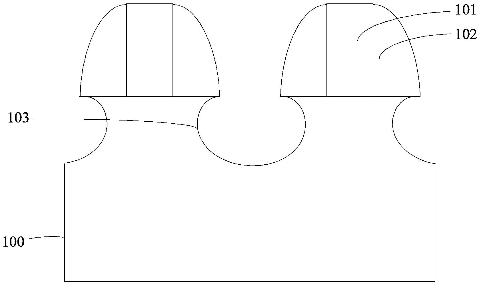
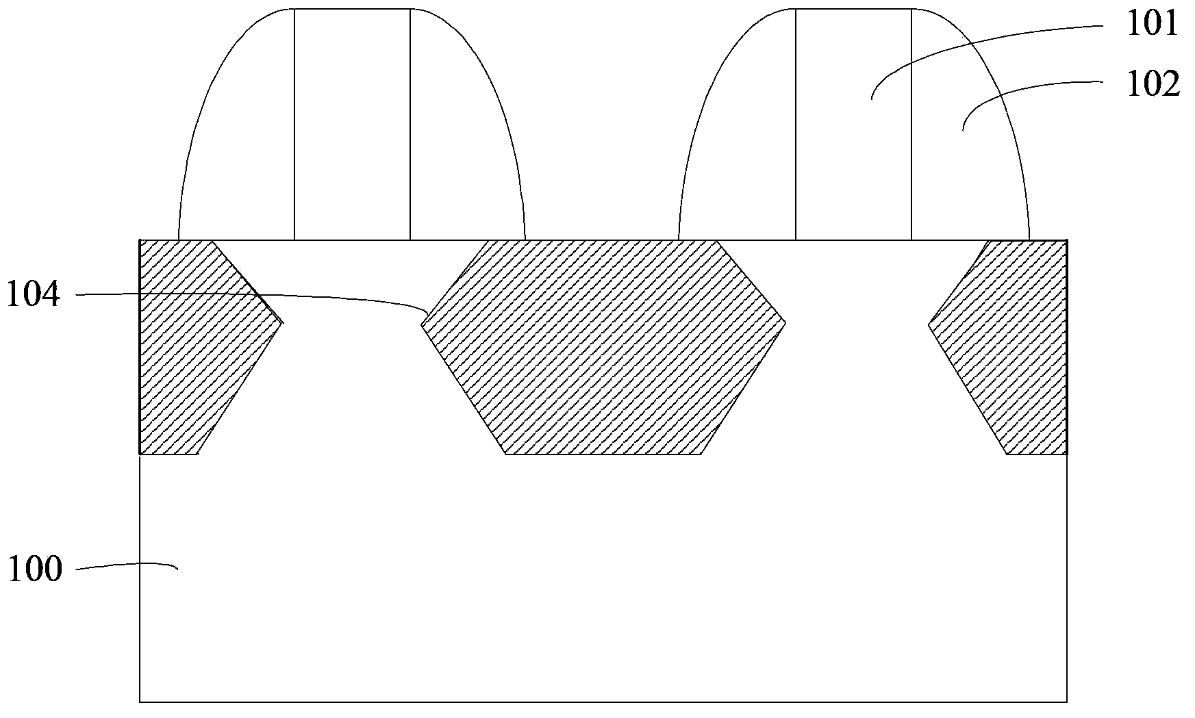
[0041] refer to figure 1 , the surface of the substrate 100 is easily oxidized in air to form an oxide (not shown in the figure), and the bottom of the sacrificial spacer 102 has the oxide. continue to refer figure 1 After the bowl-shaped groove 103 is formed, the surface of the bowl-shaped groove 103 will be oxidized in the air to form oxides. The dilute hydrofluoric acid solution can clean the oxides in the bowl-shaped groove 103 . During the process of cleaning the oxide in the bowl-shaped groove 103 , part of the oxide at the bottom of the sacrificial spacer 102 will also be removed, resulting in a gap between the sacrificial spacer 102 and the substrate. refer to figure 2 , because there is a gap between the sacrificial sidewall 102 and the substrate, when the bowl-shaped groove is etched to form the sigma-shaped groove 104, the substrate at the position o...


PUM


Abstract

The invention provides a method for manufacturing a PMOS transistor. The method includes the steps that grids are formed on a substrate, single-layer sacrifice side walls are formed around the grids, and the portions, at the bottoms of the sacrifice side walls, of the substrate are oxidized, so that oxides are formed; the sacrifice side walls serve as masks, the portions, on the two sides of each sacrifice side wall, of the substrate are etched, first grooves are formed, and the surfaces of the first grooves are exposed in air, so that oxides are formed; the oxides on the surfaces of the first grooves are removed through wet etching, the first grooves are etched so that second grooves can be formed, and part of openings of the second grooves are arranged at the bottoms of the sacrifice side walls; part of the sacrifice side walls are removed by certain thickness to the boundaries of the openings of the second grooves, and then the openings of the second grooves are completely exposed; first semiconductor materials are formed in the second grooves; second semiconductor materials are formed on the portions, between the remaining sacrifice side walls, of the substrate; the remaining sacrifice side walls are removed, side walls are formed around the grids, the side walls serve as masks, ion injection is conducted on the first semiconductor materials and the second semiconductor materials, and then source electrodes and drain electrodes are formed. By the adoption of the method, the performance of the formed PMOS transistor can be improved.

Description

technical field [0001] The invention belongs to the field of semiconductor manufacturing, in particular to a method for manufacturing a PMOS transistor. Background technique [0002] In the existing manufacturing process of semiconductor devices, since stress can change the energy gap and carrier mobility of silicon materials, it has become an increasingly common means to improve the performance of MOS transistors through stress. Specifically, by properly controlling the stress, the mobility of carriers (electrons in NMOS transistors and holes in PMOS transistors) can be increased, thereby increasing the driving current, thereby greatly improving the performance of MOS transistors. For PMOS transistors, embedded silicon germanium technology (Embedded SiGe Technology) can be used to generate compressive stress in the channel region of the transistor, thereby improving carrier mobility. The so-called embedded silicon germanium technology refers to embedding silicon germanium ...

Claims


Application Information

Patent Timeline
IPC IPC(8): H01L21/336
CPCH01L29/66568
Inventor 韩秋华隋运奇
Owner SEMICON MFG INT (SHANGHAI) CORP
Features
  • R&D
  • Intellectual Property
  • Life Sciences
  • Materials
  • Tech Scout
  • Unparalleled Data Quality
  • Higher Quality Content
  • 60% Fewer Hallucinations
Learn More