Power semiconductor device with electro-static discharging capability and manufacturing method

A power semiconductor and discharge capability technology, applied in semiconductor/solid-state device manufacturing, semiconductor devices, electric solid-state devices, etc., can solve problems such as increased cost and complex formation, and achieves high design flexibility, reduced cost, and improved ESD capability. Effect

Inactive Publication Date: 2014-11-19
HANGZHOU SILAN MICROELECTRONICS
View PDF6 Cites 0 Cited by
  • Summary
  • Abstract
  • Description
  • Claims
  • Application Information

AI Technical Summary

Problems solved by technology

However, the formation of these ESD protection components is relatively complicated, and additional masks are required, which increases the cost while improving the ESD capability
[0005] Therefore, it is necessary to propose a new power semiconductor device to solve the problem that the ESD protection component in the prior art needs to add an additional mask to improve the anti-ESD ability, and the problem of relatively complicated formation

Method used


Image

  • Power semiconductor device with electro-static discharging capability and manufacturing method
  • Power semiconductor device with electro-static discharging capability and manufacturing method
  • Power semiconductor device with electro-static discharging capability and manufacturing method

Examples


Embodiment 1

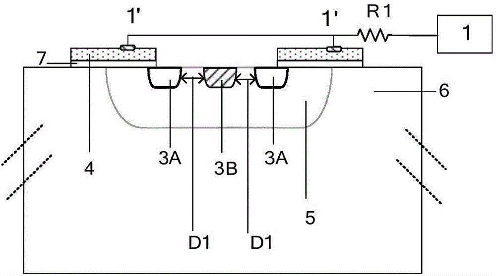
[0054] Figure 3 to Figure 5 It shows that the present invention provides a power semiconductor device with anti-static discharge capability, and the gate terminal is connected in series with strip resistors to form a circular array layout structure of the gate.

[0055] Such as Figure 3 to Figure 5 As shown, the steps for forming each of the cells 8 are as follows: provide an epitaxial layer (not shown in the figure, please refer to Figure 2A to Figure 2C In the mark 6); form a second-type lightly doped region in the epitaxial layer (not shown in the figure, please refer to Figure 2A to Figure 2C Mark 5 in the above); on the epitaxial layer, a gate dielectric layer is sequentially formed from bottom to top (not shown in the figure, please refer to Figure 2A to Figure 2C Mark 7) and the first polysilicon strip 4; etch the first polysilicon strip 4 and the gate dielectric layer to expose the second-type lightly doped region; in the second-type lightly doped A first type ...

Embodiment 2

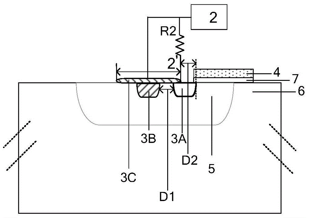
[0062] Figure 8 to Figure 9 Shown is the circular array layout structure of the source terminal of the power semiconductor device with anti-static discharge capability of the present invention, which is connected in series with strip resistors to form the source.

[0063] Such as Figure 8 with 9 As shown, the steps for forming each of the cells 8 are as follows: provide an epitaxial layer (not shown in the figure, please refer to Figure 2A to Figure 2C In the mark 6); form a second-type lightly doped region in the epitaxial layer (not shown in the figure, please refer to Figure 2A to Figure 2C Mark 5 in the above); on the epitaxial layer, a gate dielectric layer is sequentially formed from bottom to top (not shown in the figure, please refer to Figure 2A to Figure 2C Mark 7) and the first polysilicon strip 4; etch the first polysilicon strip 4 and the gate dielectric layer to expose the second-type lightly doped region; in the second-type lightly doped A first type he...

Embodiment 3

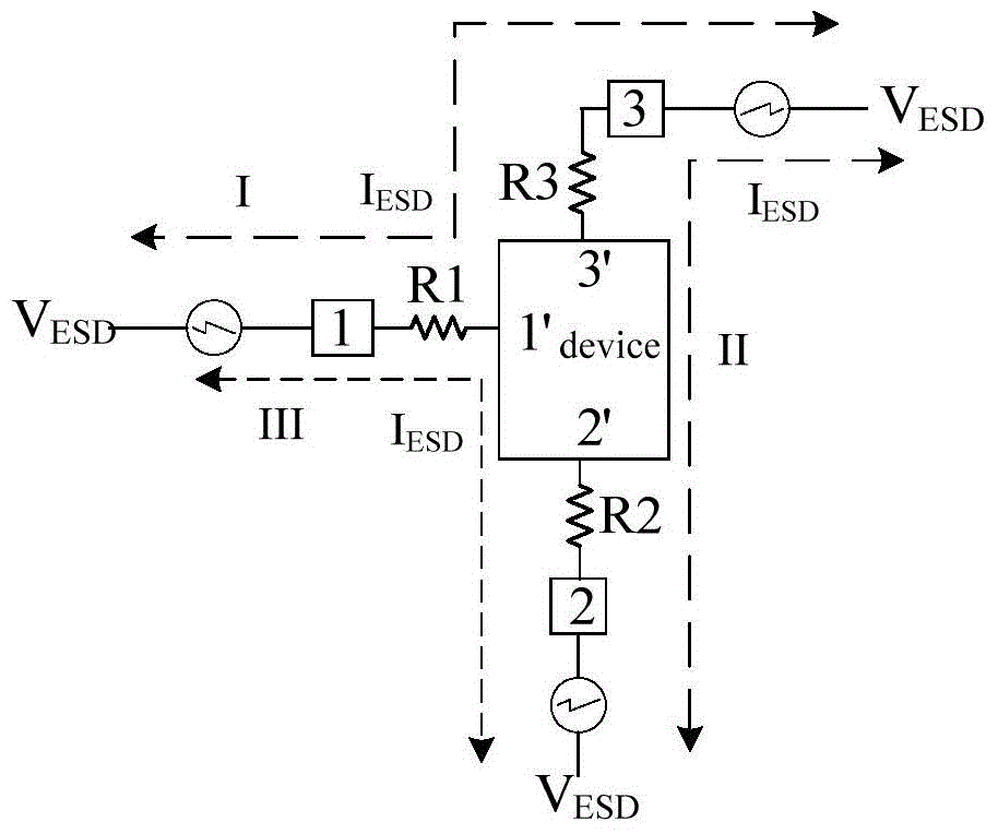
[0073] Figure 12 The difference between the illustrated embodiment and the first and second embodiments is to provide a circular array layout structure in which the gate terminal and the source terminal of the power semiconductor device with anti-static discharge capability are simultaneously connected in series with resistors to form the gate and source.

[0074] In this embodiment, the changed embodiment 1 can be combined with the layout structure of embodiment 2 to form Figure 12 . The content of the changes in the first embodiment is as follows: a first port 1' is provided on the second polysilicon strip 4', and a second port 1' is provided on the second polysilicon strip 4' other than the first port 1' The gate 1 is formed, and the second polysilicon strip 4 ′ is a resistor R1 connected to the first port, and the first port 1 ′ has no direct electrical connection with the gate 1 . Then, the size of the resistor R1 connected in series with the gate terminal can be adju...


PUM


Abstract

The application of the invention is divisional application of 201210559280.0 and discloses a manufacturing method for a power semiconductor device with electro-static discharging capability. The manufacturing method comprises the following steps: the power semiconductor with a first end, a second end and a third end is provided; the power semiconductor device is formed by arranging a cellular array; one port or multiple port of the three ports is connected with a resistor respectively to form the power semiconductor device with the electro-static discharging capability; the invention further provides the power semiconductor device with the electro-static discharging capability. According to the power semiconductor device, as the resistors connected in series with one port or multiple port of the three ports serve as ESD(Electro-Static discharge)protective components to improve the ESD capability, the capacity of the resistors connected with one port or multiple port of the three ports in series can meet the demands of the ESD in various grades through slightly adjusting a protected device layout structure and the flexibility of the design is high.

Description

[0001] The patent application of the present invention is a divisional application. The application number of the original application is 201210559280.0, and the application date is December 20, 2012. The title of the invention is: power semiconductor device with anti-static discharge capability and its manufacturing method. technical field [0002] The invention belongs to the technical field of electrostatic discharge of power semiconductor devices, and in particular relates to a power semiconductor device with anti-static discharge capability and a manufacturing method. Background technique [0003] Electrostatic Discharge (ESD) is an important factor that causes damage to most electronic components. In order to avoid damage to electronic components, electronic engineers have thought of many countermeasures. One of the mainstream ideas is to design ESD for a single device or integrated circuit , that is, by adding ESD protection components to protect the devices or integra...

Claims


Application Information

Patent Timeline
IPC IPC(8): H01L27/02H01L29/06H01L29/78H01L21/336
Inventor 叶俊张邵华
Owner HANGZHOU SILAN MICROELECTRONICS
Why Eureka
Try Eureka