Supercharge Your Innovation With Domain-Expert AI Agents!

Image sensor noise restraint full-chip ESD protection structure

An image sensor, ESD protection technology, applied in the direction of image communication, electric solid-state devices, semiconductor devices, etc., can solve problems such as short circuit, weakening the full-chip ESD protection ability of mixed-voltage image sensors, and chip failure, so as to improve stability and reliability Sex, improve protection ability, enhance the effect of protection performance

Active Publication Date: 2014-11-19
NO 771 INST OF NO 9 RES INST CHINA AEROSPACE SCI & TECH
View PDF6 Cites 3 Cited by
  • Summary
  • Abstract
  • Description
  • Claims
  • Application Information

AI Technical Summary

Problems solved by technology

Normally, the grid voltage of the reset tube of the pixel unit and the power supply voltage of each tube in the pixel unit are higher than the power supply voltage of the readout circuit and the IO circuit part of the sensor chip. The power supply ports of these high-voltage signals need special treatment. If you still use conventional IO port to supply power to these special ports, will cause if figure 2 The problem shown is that the IO port is shorted to the power rail, causing the chip to fail
Therefore, when designing a conventional mixed-voltage image sensor chip, the power rails of these high-voltage power supply IO ports will be artificially disconnected from the power rails of the sensor chip readout circuit and the power supply port of the IO circuit part, which ensures that the noise of the circuit part is not affected. It will crosstalk to the pixel unit through the power rail, and completely block the short-circuit failure problem from the electrical level, but this method also introduces Electro-Static discharge (ESD) current to discharge on the full-chip power rail and cannot form a loop. The circuit problem seriously weakens the full-chip ESD protection capability of the mixed voltage image sensor

Method used


Image

  • Image sensor noise restraint full-chip ESD protection structure
  • Image sensor noise restraint full-chip ESD protection structure
  • Image sensor noise restraint full-chip ESD protection structure

Examples


Embodiment Construction

[0033] The present invention will be further described in detail below in conjunction with specific embodiments, which are explanations of the present invention rather than limitations.

[0034] First, the image sensor noise suppression full-chip ESD protection structure and application conditions provided by the present invention are described:

[0035] (1) Unit structure

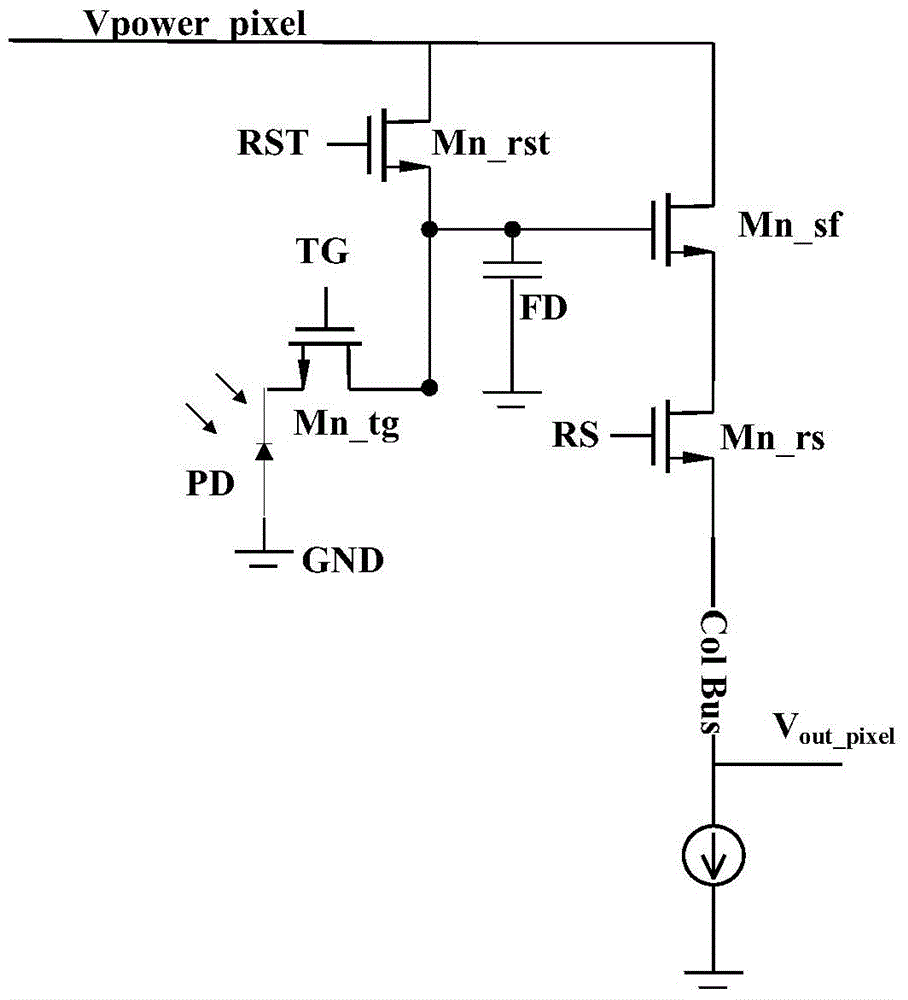
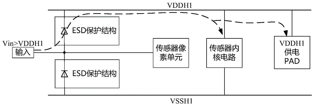
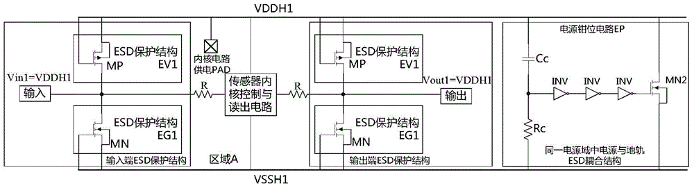
[0036] Such as image 3 As shown, the first signal input terminal and output terminal in the first area A are respectively connected to the first input and output metal pads, and the first power rail protection circuit EV1 and the first ground are connected in parallel between the first input and output metal pads The rail protection circuit EG1 protects the first power rail VDDH1 and the first ground rail VSSH1. In this preferred structure, the power clamp circuit EP is connected in series between the first power rail VDDH1 and the first ground rail VSSH1; the power clamp circuit EP connects the first A...


PUM


Abstract

The invention discloses an image sensor noise restraint full-chip ESD protection structure. The image sensor noise restraint full-chip ESD protection structure comprises a first area A and a second area B, wherein the first area A is used for supplying power to and protecting a sensor core controlling and reading circuit; the second area B is used for supplying power to and protecting a sensor pixel unit; the sensor core controlling and reading circuit is used for controlling the sensor pixel unit; the sensor pixel unit outputs collected photoelectric signals to the sensor core controlling and reading circuit; the first area A comprises a first input metal bonding pad and a first output metal bonding pad which are connected with the sensor core controlling and reading circuit, and a first power rail VDDH1 and a first ground rail VSSH1 used for supplying power; the second area B comprises a second input metal bonding pad connected with the sensor pixel unit, and a second power rail VDDH2 and a second ground rail VSSH2 used for supplying power; the first ground rail VSSH1 and the second ground rail VSSH2 are connected.

Description

technical field [0001] The invention relates to the technical field of integrated circuits, in particular to an image sensor noise suppression full-chip ESD protection structure. Background technique [0002] The currently mainstream CMOS image sensor (CIS) pixel unit is a 4T-APS structure, and its equivalent circuit is as follows figure 1 shown. It includes a reset nMOS transistor Mn_rst, a photodiode PD, an exposure control transistor Mn_tg, a source follower nMOS transistor Mn_sf for reading photoelectric signals stored in the parasitic node FD, and a row selection signal output nMOS transistor Mn_rs. Among them, the source terminal of Mn_rst is connected to the power rail Vpower_pixel, and the drain terminal is connected to FD point; the source terminal of Mn_tg is connected to PD, and the drain terminal is connected to FD; the source terminal of Mn_sf is connected to the power rail Vpower_pixel, and the drain terminal is connected to the source terminal of Mn_rs; the d...

Claims


Application Information

Patent Timeline
IPC IPC(8): H01L27/146H01L27/02H04N5/374
Inventor 张冰谭瑞李娜曹琛
Owner NO 771 INST OF NO 9 RES INST CHINA AEROSPACE SCI & TECH
Features
  • R&D
  • Intellectual Property
  • Life Sciences
  • Materials
  • Tech Scout
  • Unparalleled Data Quality
  • Higher Quality Content
  • 60% Fewer Hallucinations
Learn More