Low noise amplifier

A low-noise amplifier and amplifier technology, applied in the direction of improving the amplifier to reduce the influence of noise, etc., can solve the problem of inability to further improve the gain, and achieve the effects of low cost, improved gain performance, and increased high-frequency gain.

Active Publication Date: 2014-11-19
SHANGHAI HUAHONG GRACE SEMICON MFG CORP
View PDF2 Cites 13 Cited by
  • Summary
  • Abstract
  • Description
  • Claims
  • Application Information

AI Technical Summary

Problems solved by technology

like figure 1 The existing low-noise amplifier shown needs to set a feedback inductor at the source of the NMOS transistor M101, and further increase in gain cannot be achieved

Method used


Image

  • Low noise amplifier
  • Low noise amplifier

Examples


Embodiment Construction

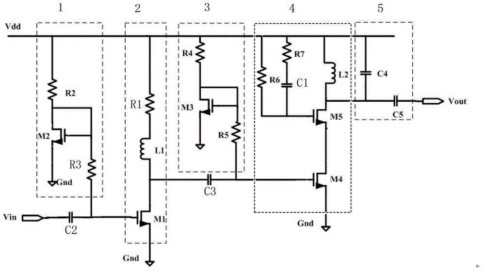
[0019] Such as figure 2 Shown is the structure diagram of the low noise amplifier of the embodiment of the present invention. The low noise amplifier in the embodiment of the present invention includes: a cascaded first-stage amplifying circuit 2 and a second-stage amplifying circuit 4 , a first-stage bias circuit 1 , a second-stage bias circuit 3 , and an output impedance matching circuit 5 .

[0020] The first-stage amplifying circuit 2 includes a first NMOS transistor M1 connected to a common source, the source of the first NMOS transistor M1 is grounded Gnd, and the drain of the first NMOS transistor M1 is connected in series with the power supply voltage Vdd. There is a first resistor R1 and a first inductor L1, the first stage bias circuit 1 provides a first bias voltage to the gate of the first NMOS transistor M1, the gate of the first NMOS transistor M1 is the The input end of the first-stage amplifying circuit 2, the drain of the first NMOS transistor M1 is used as ...


PUM


Abstract

The invention discloses a low noise amplifier. The low noise amplifier comprises a first-stage amplifying circuit, a second-stage amplifying circuit, a first-stage biasing circuit, a second-stage biasing circuit and an output impedance matching circuit, wherein the first-stage amplifying circuit and the second-stage amplifying circuit are cascaded. The first-stage amplifying circuit comprises first NMOS pipes with the common sources connected, and a first resistor and a first inductor are connected between the drain electrodes of the first NMOS pipes and a supply voltage. The second-stage amplifying circuit comprises a cascode CMOS amplifier. According to the low noise amplifier, the first-stage amplifying circuit and the second-stage amplifying circuit are cascaded so that the gain performance and the noise performance of the circuits can be greatly improved; a first inductive load at the drain end of the first-stage amplifying circuit enables the total impedance of the load end of the first-stage amplifying circuit to keep roughly unchangeable within a wide frequency range, and therefore the high frequency gain of the whole circuit can be improved and can be stable; the cascode amplifier is adopted in the second-stage amplifying circuit so that the whole low noise amplifier can obtain the good noise performance and gain performance.

Description

technical field [0001] The invention relates to a semiconductor integrated circuit, in particular to a low noise amplifier. Background technique [0002] In the prior art, low noise amplifiers generally adopt RF CMOS process design, such as figure 1 As shown, it is a structural diagram of an existing low-noise amplifier designed using RF CMOS technology. NMOS transistor M101 and NMOS transistor M102 form a source feedback cascode amplifier circuit. Resistor R101, resistor Rb and NMOS transistor M103 are NMOS The transistor M101 provides a bias voltage, wherein the NMOS transistor M103 and the NMOS transistor M101 form a current mirror structure and implement a bias to the NMOS transistor M101. The source of the MNOS transistor M101 is grounded through the feedback inductance Ls, an input resonant network is formed between the feedback inductance Ls and the gate-source capacitance Cgs1 of the NMOS transistor M101, and a real impedance is obtained to achieve input impedance m...

Claims


Application Information

Patent Timeline
Patent Type & Authority Applications(China)
IPC IPC(8): H03F1/26
Inventor 朱红卫唐敏刘国军赵郁炜
Owner SHANGHAI HUAHONG GRACE SEMICON MFG CORP
Why Eureka
Try Eureka