Trench gate IGBT chip

A trench gate and chip technology, applied in electrical components, circuits, semiconductor devices, etc., can solve the problems of increasing the difficulty and cost of the IGBT chip process, increasing the number of virtual gates, etc., and achieve the effect of increasing the trench density and improving the withstand voltage

Active Publication Date: 2014-12-03
ZHUZHOU CRRC TIMES SEMICON CO LTD
View PDF5 Cites 17 Cited by
  • Summary
  • Abstract
  • Description
  • Claims
  • Application Information

AI Technical Summary

Problems solved by technology

[0005] Continue to increase the number of dummy gates on the outside of the conventional gate along the direction of the original dummy gate: In the case of constant cell size, increasing the number of dummy gates outside the conventional gate means that the process feature size ...

Method used


Image

  • Trench gate IGBT chip
  • Trench gate IGBT chip
  • Trench gate IGBT chip

Examples


Embodiment 1

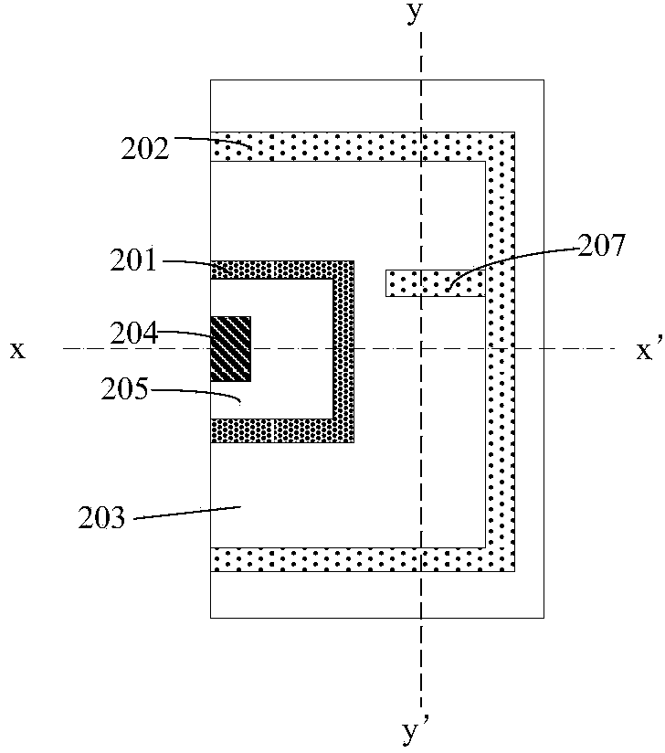
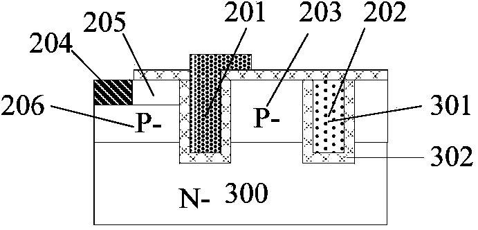
[0041] figure 2 It is a schematic plan view of the half-cell structure of the trench gate IGBT chip provided by Embodiment 1 of the present invention, and FIG. 3(a) is figure 2 The schematic cross-sectional view along the x-x' direction of the half-cell structure of the trench gate IGBT chip shown in Figure 3(b) is figure 2 The schematic cross-sectional view along the y-y' direction of the half-cell structure of the trench gate IGBT chip shown.

[0042] It should be noted that the trench gate IGBT chip described in Embodiment 1 is described by taking an N-type substrate material as an example.

[0043] like figure 2 As shown, the half-cell structure of the trench gate IGBT chip provided by Embodiment 1 of the present invention includes the first trench gate 201 and the second trench gate 202, between the first trench gate 201 and the second trench gate 202 isolated by the P-type region 203 . The half-cell structure further includes an emitter 204 and an N+ source region ...

Embodiment 2

[0059] The cellular structure of the trench gate IGBT chip described in Embodiment 2 has many similarities with the cellular structure of the trench gate IGBT chip described in Embodiment 1. For the sake of brevity, this embodiment only has the differences Make an emphatic explanation.

[0060] Figure 4 It is a schematic plan view of the half-cell structure of the trench gate IGBT chip provided by Embodiment 2 of the present invention, and FIG. 5(a) is Figure 4 The schematic cross-sectional view along the x-x' direction of the half-cell structure of the trench gate IGBT chip shown in Figure 5(b) is Figure 4 The schematic cross-sectional view along the y-y' direction of the half-cell structure of the trench gate IGBT chip shown.

[0061] like Figure 4 As shown, the half-cell structure of the trench gate IGBT chip described in the second embodiment includes three II trench gates 202 and four III trench gates 207, and the II trench gates 202 are respectively II -1 trench ...

Embodiment 3

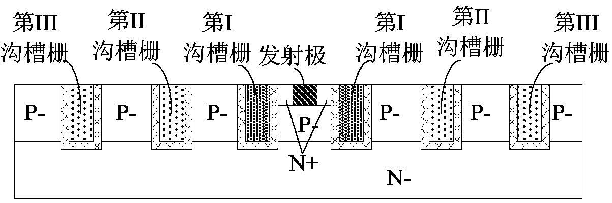
[0071] When the P-type sub-region is in a floating state, the turn-off speed will be reduced, and the turn-off loss will be increased, which will affect the performance of the safe working area of ​​the chip. Therefore, it is necessary to lead out the P-type sub-region to the surface of the chip to realize an electrical ground connection. However, when the dummy gate trench gate forms a network structure, each P-type sub-region formed by division is isolated from each other. If each P-type sub-region is electrically connected to ground, according to the traditional method, it is necessary to connect each P-type sub-region to the ground. A lead-out window for leading the P-type sub-region to the chip surface is set on the suspended P-type sub-region, which will lead to a reduction in the number of grooves per unit area due to the existence of the lead-out window under the limitation of equipment and process level , that is, reducing the trench density, which is not conducive to...


PUM

PropertyMeasurementUnit
Doping concentrationaaaaaaaaaa

Abstract

The invention provides a trench gate IGBT chip. The trench gate IGBT chip comprises a plurality of cells connected in parallel, each cell comprises a first trench gate and a second trench gate, each first trench gate and the corresponding second trench gate are isolated through a first conduction type region, each second trench gate is located on one side of the corresponding first trench gate, and an emitter and a second conduction type source electrode region are arranged on the other side of the corresponding first trench gate. The trench gate IGBT chip further comprises third trench gates formed in the first conduction type region, and the straight line where the gate lengths of the third trench gates are located is intersected with the straight line where the gate lengths of the second trench gates are located. Compared with the prior art, the trench gate IGBT chip has the advantages that technology difficulty and technology cost for manufacturing cannot be increased. In addition, as the third trench gates are additionally arranged, the trench density of the trench gate IGBT chip is improved, voltage withstanding of the trench gate IGBT chip is easily improved, power dissipation of the trench gate IGBT chip is easily reduced, and the safety working area performance of the trench gate IGBT chip is easily improved.

Description

technical field [0001] The invention relates to the field of semiconductor devices, in particular to a trench gate IGBT chip. Background technique [0002] At present, most IGBT manufacturers adopt trench gate structure technology to obtain lower power consumption, higher power density, and faster switching speed. [0003] For trench gate IGBT chips, trench gate IGBT chips with dummy gates appear now in order to take into account the withstand voltage, power consumption and safe operating area performance of the chip. In the structure of the IGBT chip, the gate is divided into a normal gate and a dummy gate. Conventional gates are used for switch control, while virtual gates are used to improve chip performance (such as on-resistance, withstand voltage and safe operating area, etc.). A schematic cross-sectional view of a trench gate IGBT chip with a dummy gate is shown in figure 1 shown. exist figure 1 The cell structure of the shown IGBT chip includes groove I, groove ...

Claims


Application Information

Patent Timeline
IPC IPC(8): H01L29/739H01L29/06
CPCH01L29/66348H01L29/7397
Inventor 刘国友覃荣震黄建伟
Owner ZHUZHOU CRRC TIMES SEMICON CO LTD
Why Eureka
Try Eureka