
A kind of semiconductor device and its forming method

A semiconductor and device technology, applied in the field of semiconductor devices and their manufacturing processes, can solve problems such as charge balance deterioration

Active Publication Date: 2017-06-06
SHANGHAI HUAHONG GRACE SEMICON MFG CORP
View PDF7 Cites 0 Cited by
  • Summary
  • Abstract
  • Description
  • Claims
  • Application Information

AI Technical Summary

Problems solved by technology

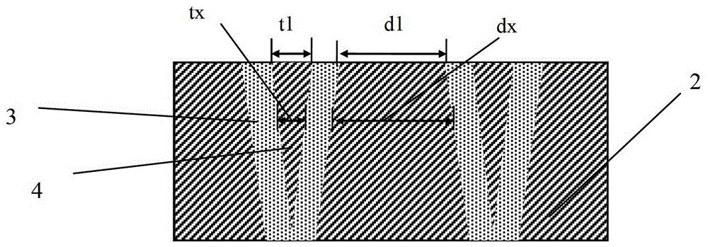
However, this technology brings certain negative effects, that is, after the trench filling is completed, the vertical width distribution trend of the P-pillar and N-pillar is opposite, that is, the P-pillar gradually narrows from top to bottom, while the N-pillar (corresponding to the P-pillar part) gradually widens from top to bottom, causing a deterioration of the charge balance (see Figure 4 )

Method used


Image

  • A kind of semiconductor device and its forming method
  • A kind of semiconductor device and its forming method
  • A kind of semiconductor device and its forming method

Examples


Embodiment 1

[0050] Such as Figure 3a-Figure 3f Shown, the technological process of this embodiment 1 is specifically as follows:

[0051] 1) The first semiconductor layer 2 and the dielectric layer 15 are sequentially grown on the semiconductor substrate 1, the first semiconductor layer 2 and the semiconductor substrate 1 have the first conductivity type, and the first semiconductor layer 2 and the semiconductor substrate 1 are made of Si, C, Ge , SiC, GaN or SiGe single crystal material, a typical first semiconductor layer 2 is an N-type silicon epitaxial layer, a typical semiconductor substrate 1 is an N-type silicon substrate, and the carrier concentration of the semiconductor substrate 1 is greater than that of the first semiconductor layer 2; the thickness of the first semiconductor layer 2 is 10-100 microns; the dielectric layer 15 is at least one of silicon oxide, silicon nitride or silicon oxynitride (see Figure 3a );

[0052] 2) Trench etching. A groove 16 is etched inside t...

Embodiment 2

[0068] The difference between Embodiment 2 and Embodiment 1 is that the conductivity types are opposite. In Embodiment 2, the first conductivity type is P-type, and the second conductivity type is N-type. That is, the semiconductor substrate 1 , the first semiconductor layer 2 , and the third semiconductor layer 4 in Embodiment 2 are P-type, the second semiconductor layer 3 is N-type, the base region 5 is N-type, and the source region 6 is P-type.


PUM


Abstract

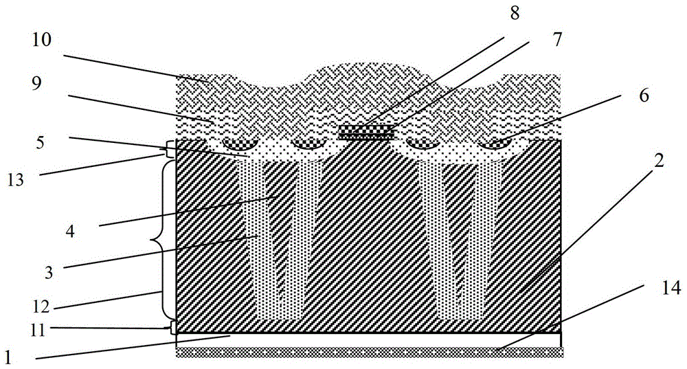
Disclosed in the invention is a semiconductor device comprising a semiconductor substrate, a semiconductor drift region, base electrode regions, source regions, a grid dielectric layer, a grid electrode, metal pre dielectric layers, and a second electrode. To be specific, a first electrode is formed at one side of the semiconductor substrate. The semiconductor drift region is formed by a first drift region, a second drift region, and a third drift region; and the first drift region, the second drift region, and the third drift region are stacked at the other side of the semiconductor substrate upwardly in sequence. The base electrode regions are formed inside the third drift region. The source regions are formed inside the base electrode region. The grid dielectric layer is formed on the third drift region and is located between the two base electrode regions. The grid electrode is formed on the grid dielectric layer. The metal pre dielectric layers are formed around the grid electrode and at the top of the third drift region except the portion between the two source regions. The second electrode is formed on the grid electrode, the metal pre dielectric layers, and the third drift region between the two source regions. In addition, the invention also discloses a forming method of the semiconductor device. Therefore, the charge balance capability of the super junction drift region can be effectively improved.

Description

technical field [0001] The invention belongs to the manufacturing process of semiconductor integrated circuits, and relates to a semiconductor device and a manufacturing process method thereof. Background technique [0002] VDMOSFET (Vertical Double-diffused MOSFET, vertical double-diffused MOS transistor) can reduce the on-resistance by reducing the thickness of the drain drift region. However, reducing the thickness of the drain drift region will reduce the breakdown voltage of the device. Therefore, in VDMOS, increasing the breakdown voltage of the device and reducing the on-resistance of the device are a pair of contradictions. The super-junction MOSFET adopts a new voltage-resistant layer structure - using a series of alternately arranged P-type and N-type semiconductor thin layers to deplete the P-type and N-type regions under the reverse voltage at a lower voltage to achieve mutual charge compensation. As a result, the P-type and N-type regions can achieve high break...

Claims


Application Information

Patent Timeline
Patent Type & Authority Patents(China)
IPC IPC(8): H01L29/78H01L29/06H01L21/336
CPCH01L29/0688H01L29/66477H01L29/7834
Inventor 刘继全
Owner SHANGHAI HUAHONG GRACE SEMICON MFG CORP
Learn More