

Multi-chip LED packaging method based on aluminum matrix composite substrate
An aluminum-based composite material, LED packaging technology, applied in electrical components, electric solid-state devices, circuits, etc., can solve problems such as uncollected data and no discovery, achieve compact structure, reduce thermal stress, and ensure thermal matching. sexual effect
Inactive Publication Date: 2014-12-03
SHANGHAI SPACEFLIGHT INST OF TT&C & TELECOMM
View PDF6 Cites 11 Cited by
- Summary
- Abstract
- Description
- Claims
- Application Information
AI Technical Summary
Problems solved by technology
At present, there is no description or report of similar technology to the present invention in China, and no similar information has been collected at home and abroad.
Method used
View moreImage
Smart ImageViewing Examples


Examples
Embodiment approach
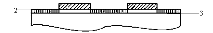
[0031] By adopting the second implementation mode of the present invention, the multi-chip LED packaging of the aluminum-based composite material substrate can be realized more reliably, and its stability can be further improved.
Login to View More PUM
| Property | Measurement | Unit |
|---|---|---|
| thickness | aaaaa | aaaaa |
Abstract
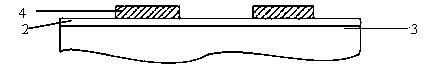
The invention relates to a multi-chip LED packaging method based on an aluminum matrix composite substrate. The method comprises the steps that aluminum matrix composite material with high heat conductivity is adopted to act as a substrate. A layer of aluminum film is grown on the substrate, and a multi-hole type aluminum oxide layer is generated via performance of selective anodic oxidation on the substrate. Then a conductor wiring and electrode welding region is manufactured via a thin film technology, and then micro assembling and micro interconnection of LED chips are performed and finally packaging of a transparent shell is performed. A heat radiation problem of the LED chips is solved. Heat can be directly transmitted to the aluminum matrix composite substrate to be radiated out via a multi-hole type heat-radiating channel so that a heat-radiating path is greatly shortened and heat radiation effect is great.
Description
[0001] technical field [0002] The invention relates to a multi-chip LED packaging method based on an aluminum anodic oxidation technology, in particular to a multi-chip LED packaging method based on an aluminum-based composite material substrate, which belongs to the field of LED packaging. Background technique [0003] LED (Light Emitting Diode) is a solid-state semiconductor device that can directly convert electrical energy into light energy. LED packaging technology is mostly developed and evolved on the basis of discrete device packaging technology, but it has great particularity. Generally, the die of a discrete device is sealed in a package, and the function of the package is mainly to protect the die and complete electrical interconnection. The LED package is to ensure the electrical and mechanical contact between the light-emitting chip and the circuit, and to protect the light-emitting chip from mechanical, heat, humidity and other external influences, while out...
Claims
Login to View More Application Information
Patent Timeline
 Patent Type & Authority Applications(China)
IPC IPC(8): H01L33/48H01L33/62H01L33/64H01L25/075H01L21/60
CPCH01L2224/48091H01L2924/00014H01L33/647H01L33/62H01L2933/0066H01L2933/0075
Inventor 杨旭一任颖丹王立春王盈莹符容
Owner SHANGHAI SPACEFLIGHT INST OF TT&C & TELECOMM