

Fine-line PCB manufacturing method
A technology of fine lines and production methods, which is applied in the direction of removing conductive materials by chemical/electrolytic methods, and can solve the problems of fine line side erosion and excessive side erosion of fine lines, so as to reduce the amount of side erosion, ensure production quality, Avoid the effect of collapse
- Summary
- Abstract
- Description
- Claims
- Application Information
AI Technical Summary
Problems solved by technology
Method used
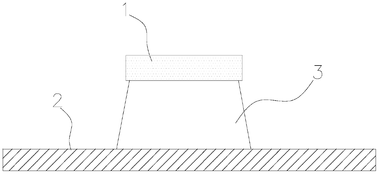
Image

Examples
Embodiment 1
[0020] A method for manufacturing a fine circuit PCB provided in this embodiment includes the following steps:
[0021] (1) Lay the inner layer circuit board, prepreg and copper foil with a thickness of 2OZ in sequence according to the requirements, and put the smooth side of the copper foil inward and the rough side outward, that is, the smooth side of the copper foil faces the prepreg to form a stack Plywood.
[0022] Then the laminated boards are moved into a press furnace and pressed together by a hot pressing process to form a multi-layer board. During the hot pressing process, the temperature and pressure gradually change with time as shown in the table below, and the total time is 280 minutes:
[0023] temperature
140
165
185
210
195
195
195
175
140
140
pressure
50
250
250
400
400
400
200
200
100
100
time
8
7
9
40
15
70
30
20
18 ...
Embodiment 2
[0033] A conventional manufacturing method of a fine circuit PCB provided in this embodiment includes the following steps:
[0034] (1) Lay the inner layer circuit board, prepreg and copper foil with a thickness of 0.25OZ (the thinnest copper foil in the industry) in order according to the requirements, and put the rough side of the copper foil inward and the smooth side outward, that is, copper The matte side of the foil faces the prepreg to form a laminate.
[0035] Then the laminated boards are moved into a press furnace and pressed together by a hot pressing process to form a multi-layer board. During the hot pressing process, the temperature and pressure gradually change with time as shown in the table below, and the total time is 280 minutes:
[0036] temperature
140
165
185
210
195
195
195
175
140
140
pressure
50
250
250
400
400
400
200
200
100
100
time
8
7...
Embodiment 3
[0045]This embodiment is basically the same as Embodiment 1, except that the thickness of the copper foil used in the step (1) of this embodiment is 3OZ.
[0046] Using copper foil with 3OZ copper thickness, the drill tip will be damaged during the drilling process, and the life of the drill tip will be shortened, and the production cost of the fine line PCB will increase due to the thicker copper foil.
PUM
 Abstract
Description
Claims
Application Information