Method for efficiently producing high-precision multistep microlens array

A micro-lens array, high-precision technology, which is applied to lenses, micro-lithography exposure equipment, photolithography process exposure devices, etc., can solve the problems of long production time and high cost, save production costs, save costs, and improve production efficiency. Effect

Active Publication Date: 2014-12-24
中航凯迈上海红外科技有限公司
View PDF6 Cites 9 Cited by
  • Summary
  • Abstract
  • Description
  • Claims
  • Application Information

AI Technical Summary

Problems solved by technology

[0007] The purpose of the present invention is to provide a method for making a multi-step microlens array, in order to solve the problems of long production time and high cost of existing production methods

Method used


Image

  • Method for efficiently producing high-precision multistep microlens array
  • Method for efficiently producing high-precision multistep microlens array
  • Method for efficiently producing high-precision multistep microlens array

Examples


Embodiment 1

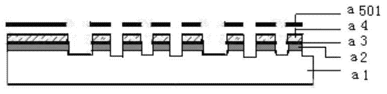
[0039] The present invention provides a method for ingeniously manufacturing a multi-step microlens array, which is applied to a sixteen-step silicon microlens array. The specific implementation scheme includes:

[0040] 1.1.1, one etching, see figure 1 .

[0041] 1) Clean the silicon substrate a1, spin-coat a layer of sacrificial layer a2, then grow a chromium film a3, and finally spin-coat a layer of positive photoresist a4;

[0042] 2) Photolithographic development is carried out with the mask plate a501, where the mask plate a501 includes eight annular zones, and the photoresist exposure and development area is equal to the dry etching area;

[0043] 3) removing the chromium film a3 on the surface of the silicon substrate a1, and cleaning the positive photoresist a4;

[0044] 4) Etching the sacrificial layer a2 to expose the region that needs to be dry-etched, performing one-time etching by dry-etching technology, and taking out the silicon substrate a1 after etching. ...

Embodiment 2

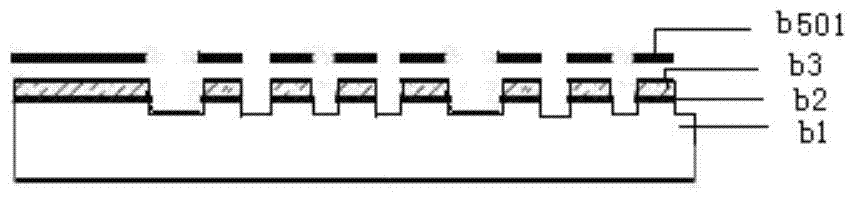
[0078] The present invention provides a method for ingeniously manufacturing a multi-step microlens array, which is applied to a sixteen-step quartz microlens array. The specific implementation scheme includes:

[0079] 2.1.1, one etching, see Figure 11 .

[0080] 1) Clean the quartz substrate b1, grow the chromium film b2, and then spin-coat a layer of positive photoresist b4;

[0081] 2) Photolithographic development is carried out with the mask b501, where the mask b501 includes eight annular zones, and the photoresist exposure and development area is equal to the dry etching area;

[0082] 3) removing the chromium film b2 on the surface of the quartz substrate b1, and cleaning the positive photoresist b3;

[0083] 4) Etching the area to be dry-etched once using dry etching technology, and taking out the quartz substrate b1 after etching.

[0084] 2.1.2, secondary etching, please refer to Figure 12 .

[0085] 1) Clean the quartz substrate b1 first, and spin-coat a la...

Embodiment 3

[0116] The present invention provides a method for ingeniously manufacturing a multi-step microlens array, which is applied to an eleven-step microlens array, and only needs to retain the manufacturing technology of eleven steps and below, and remove the manufacturing technology of more than eleven steps. In a specific embodiment, the mask plate 501a or 501b only includes five rings in the first etching; the mask 502a or 502b only includes two rings in the second etching; the mask 503a in the third etching Or 503b only includes three rings; the mask plate 504a or 504b only includes three rings in four etchings; the mask 505a or 505b only includes one ring in five etchings; The stencil 506a or 506b only includes two rings; the mask 507a or 507b only includes one ring in the seven etchings, and other processes are similar to those in Embodiment 1.


PUM


Abstract

The invention relates to a method for efficiently producing a high-precision multistep microlens array. The method includes that the step array to be produced is divided into multiple groups including a first group and a second group, the first group and the second group are connected end to end, and steps of each group are continuous in depth; the steps of the first group and the second group are synchronously produced to form two groups of steps identical in corresponding depth; the steps in the second group are integrally etched by certain depth and form the step array continuous in depth with the steps in the first group. By the method, the steps in different groups are created synchronously, so that producing efficiency is greatly improved, and cost is saved.

Description

technical field [0001] The invention relates to a method for making a multi-step microlens array. Background technique [0002] The microlens array is an array composed of a series of tiny lenses with diameters of millimeters and micrometers in a certain arrangement. Micro-lenses and micro-lens arrays produced by micro-optical technology have become a new direction of scientific research and development due to their advantages of small size, light weight, easy integration, and arraying. [0003] With the rapid development of modern information technology, the application of microlenses in various fields is becoming more and more extensive. From the current point of view, microlenses play a pivotal role in both military and civilian applications. In some developed countries such as Japan, the United States, the United Kingdom, and Germany, the research on microlenses has attracted great attention from government departments, and they are competing to invest in the developme...

Claims


Application Information

Patent Timeline
Patent Type & Authority Applications(China)
IPC IPC(8): G02B3/00G03F7/20
Inventor 侯治锦司俊杰韩德宽陈洪许吕衍秋王巍
Owner 中航凯迈上海红外科技有限公司
Why Eureka
Try Eureka