SiC metal oxide semiconductor field effect transistor and production method thereof

A technology of oxide semiconductors and transistors, applied in semiconductor/solid-state device manufacturing, semiconductor devices, electrical components, etc., can solve problems such as complex, difficult breakdown voltage and conduction characteristics, to protect device terminals and reduce adverse effects The possibility of factors, the effect of reducing the complexity of device design

Active Publication Date: 2014-12-24
INST OF MICROELECTRONICS CHINESE ACAD OF SCI
View PDF5 Cites 12 Cited by
  • Summary
  • Abstract
  • Description
  • Claims
  • Application Information

AI Technical Summary

Problems solved by technology

[0007] The purpose of the present invention is to address the above-mentioned deficiencies in the prior art and combine the current SiC material technology problems to propose a SiC metal oxide semiconductor transistor and its manufacturing method to solve the complex and difficult design of the P well and terminal structure in the preparation of SiC MOSFET devices. Simultaneously realize the optimization problem of breakdown voltage and conduction characteristics, achieve the purpose of simplifying the design and improving the comprehensive performance of SiC MOSFET devices

Method used


Image

  • SiC metal oxide semiconductor field effect transistor and production method thereof
  • SiC metal oxide semiconductor field effect transistor and production method thereof
  • SiC metal oxide semiconductor field effect transistor and production method thereof

Examples


Embodiment Construction

[0051] In order to make the object, technical solution and advantages of the present invention clearer, the present invention will be described in further detail below in conjunction with specific embodiments and with reference to the accompanying drawings.

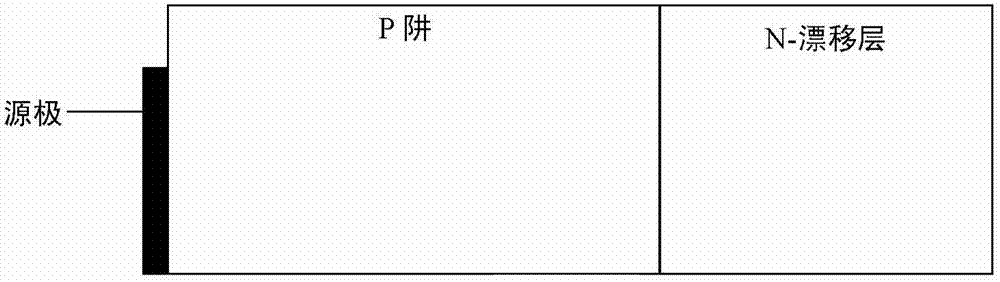
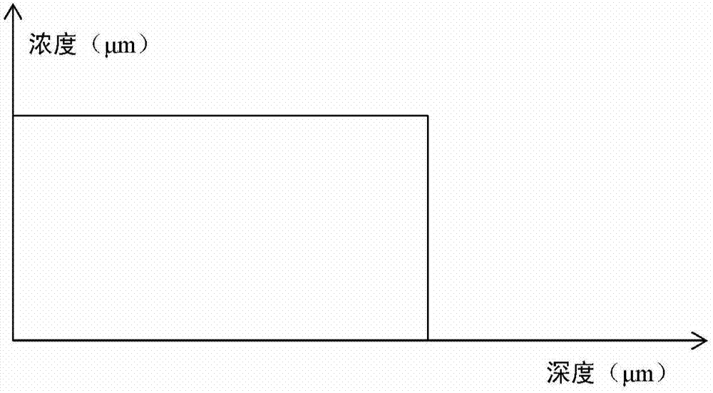
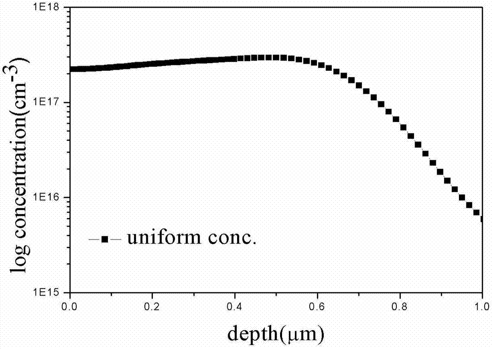
[0052] The SiC metal-oxide-semiconductor transistor and its manufacturing method proposed by the present invention, for the P-well, use less energy combination to realize a slowly increasing concentration gradient, while taking into account the withstand voltage and conduction characteristics of the device; for the terminal structure, use The P-well in the cell area is expanded to form the main junction of the terminal structure; the field-limiting ring area uses P + Combined with the P well, high voltage design is realized, and the P + The design of the P well is consistent with the cell area, and its implantation is formed when the cell is implanted, which simplifies the implantation process steps of the field limit rin...


PUM


Abstract

The invention discloses an SiC metal oxide semiconductor field effect transistor and a production method thereof. The SiC metal oxide semiconductor transistor comprises a source electrode, a gate electrode, an SiO2 oxide media dielectric, an N+ source region, a P+ contact region, an optimized doped P well, an optimized doped main junction, an N- epitaxial layer, a buffer layer, an N+ substrate, a drain electrode, optimized doped field limiting rings, a cut-off region and an isolation dielectric. According to the production method of the SiC metal oxide semiconductor field effect transistor, the SiC metal oxide semiconductor field effect transistor of a P- well and terminal structure in optimized concentration distribution is formed by means of Al injection with less energy integration, the production process is relatively simple, and conduction and breakdown characteristics of the transistor are taken into consideration. The SiC metal oxide semiconductor field effect transistor produced by the method can be used for power-switch power supply circuits, DC / DC, AC / DC and DC / AC converters and the like.

Description

technical field [0001] The invention relates to the technical field of SiC metal-oxide-semiconductor transistors, in particular to a SiC metal-oxide-semiconductor transistor and a SiC metal-oxide-semiconductor transistor having both high breakdown and low conduction characteristics and simplified process steps by using an optimized P well and terminal Al ion implantation process. Production Method. Background technique [0002] Silicon carbide material has excellent physical and electrical properties. With its unique advantages such as wide band gap, high thermal conductivity, large saturation drift velocity and high critical breakdown electric field, it has become a high-power, high-frequency, durable It is an ideal semiconductor material for high-temperature and radiation-resistant devices, and has broad application prospects in military and civil affairs. Power electronic devices made of SiC materials have become one of the hot devices and frontier research fields in the...

Claims


Application Information

Patent Timeline
Patent Type & Authority Applications(China)
IPC IPC(8): H01L29/06H01L29/78H01L21/04
CPCH01L29/66666H01L29/7869H01L21/265H01L29/7811H01L29/0619H01L29/66068H01L29/1608
Inventor 霍瑞彬申华军白云
Owner INST OF MICROELECTRONICS CHINESE ACAD OF SCI
Why Eureka
Try Eureka