
Power mosfet device with low characteristic on-resistance and method of manufacturing the same

A technology of on-resistance and devices, which is applied in the field of power semiconductor devices, can solve problems such as increasing manufacturing costs, reducing product reliability, and hidden dangers of reliability, so as to reduce manufacturing difficulty and cost, increase gate oxide withstand voltage quality, and reduce drive voltage. The effect of loss

Active Publication Date: 2017-02-01
WUXI NCE POWER
View PDF5 Cites 0 Cited by
  • Summary
  • Abstract
  • Description
  • Claims
  • Application Information

AI Technical Summary

Problems solved by technology

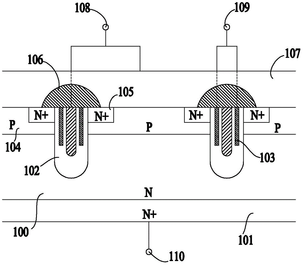
[0008] 2. Since the conductive polysilicon connected to the gate and the conductive polysilicon connected to the source in the cell trench are separated by an insulating oxide layer, the reliability of the isolation must be considered. In the actual manufacturing process, These two parts of conductive polysilicon need to undergo polycrystalline etching. It is difficult to make the appearance of polysilicon after etching smooth and tidy. There are usually some sharp corners or "V"-shaped shallow grooves. Therefore, after the growth of the insulating oxide layer It is also difficult to achieve a uniform and flat thickness, which brings huge hidden dangers to future reliability. Facts have proved that this problem has become one of the main risk points of this type of structure
[0009] 3. Since two parts of conductive polysilicon isolated from each other are to be formed in the same trench, the process steps such as trench etching, thick oxide layer growth and corrosion, polysilicon deposition and etching often restrict each other. window, thus greatly increasing the complexity of the process, which not only reduces the reliability of the product, but also increases the manufacturing cost
[0010] 4. Since the conductive polysilicon connected to the source is located in the lower half of the trench, and this part of the conductive polysilicon needs to be extracted and connected to the source, this structure also increases the design difficulty and window of the device, and will also increase to a certain extent Die area and manufacturing complexity of the device

Method used


Image

  • Power mosfet device with low characteristic on-resistance and method of manufacturing the same
  • Power mosfet device with low characteristic on-resistance and method of manufacturing the same
  • Power mosfet device with low characteristic on-resistance and method of manufacturing the same

Examples


Embodiment Construction

[0069] The present invention will be further described below in conjunction with specific drawings and embodiments.

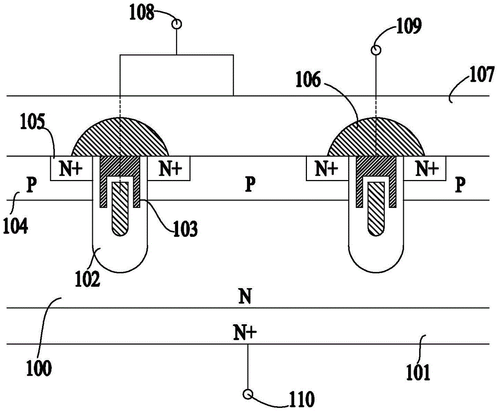
[0070] Such as figure 1 Shown: is the implementation structure diagram of the existing trench power MOSFET device with low characteristic on-resistance, in which, on the cross-section of the power MOSFET device, the element area of ​​the power MOSFET device adopts a trench structure, and the cell trench is located in In the N-type drift region 100 , the depth of the cell trench is smaller than the thickness of the N-type drift region 100 , and the N-type drift region 100 is adjacent to the N+ substrate region 101 . A P-type well region 104 is provided in the upper part of the N-type drift region 100 , and the P-type well region 104 runs through the N-type drift region 100 . A trench insulating oxide layer 102 and a trench polysilicon 103 are arranged in the cell trench, and an N+ cell implantation region 105 is arranged outside the notch of the cell trench, an...


PUM


Abstract

The invention relates to a power MOSFT (metal-oxide -semiconductor field effect transistor) device with low specific on-resistance and a manufacturing method of the power MOSFT device. An element region of the power MOSFT device comprises first trenches and second trenches which are arranged alternatively; depth of each of the second trenches in a first conductive type drift layer is not larger than that of each of the first trenches in the first conductive type drift layer. The first trenches which are covered with insulated oxide layers are filled with first conductive polycrystalline silicon; the second trenches which are covered with insulated gate oxide layers are filled with second conductive polycrystalline silicon. First conductive type injection regions are arranged on two sides of the opening of each of the second trench; the openings of the second trenches are covered with insulated dielectric layers. A first main surface metal layer is electrically simultaneously connected with the first conductive type injection regions and second conductive type well layers under the first main surface. The power MOSFT device has the advantages of low on-resistance, small gate charge (Qg), simple manufacturing process and high reliability.

Description

technical field [0001] The invention relates to a power MOSFET and a manufacturing method thereof, in particular to a power MOSFET with low characteristic on-resistance and a manufacturing method thereof, belonging to the technical field of power semiconductor devices. Background technique [0002] The characteristic on-resistance (Rsp) is one of the most important indicators for evaluating the current conduction capability of a MOSFET device. Usually, the product of the characteristic on-resistance and the charge on the gate (Qg) or the charge on the gate-drain electrode (Qgd) (ie, Rsp *Qg or Rsp*Qgd) is used as the quality factor (FOM) of the device. The quality factor becomes the most direct and important technical indicator for judging the overall performance of a MOSFET product. The smaller the FOM, the lower the power loss of the device. [0003] For 500V to 900V medium and high voltage MOSFET devices, the use of super junction technology (Super Junction) can effective...

Claims


Application Information

Patent Timeline
Patent Type & Authority Patents(China)
IPC IPC(8): H01L29/78H01L29/423H01L29/06
CPCH01L29/66727H01L29/66734H01L29/7813H01L29/7833H01L29/7835
Inventor 朱袁正叶鹏
Owner WUXI NCE POWER
Learn More