Patterning method using laser etching
A laser etching and patterning technology, which is applied in the manufacture of electrical components, circuits, semiconductors/solid-state devices, etc., can solve problems such as the visibility of transparent electrodes, and achieve visibility problems, excellent pattern resolution, and realization of The effect of fine line width
- Summary
- Abstract
- Description
- Claims
- Application Information
AI Technical Summary
Problems solved by technology
Method used
Image

Examples
manufacture example 1
[0039] Manufacturing example 1 (formation of metal nanowire layer)
[0040] Metal nanowires and additives in various weight ratios are added to pure water to make them uniformly dispersed and fully mixed to manufacture metal nanowire inks for transparent electrodes. Use the manufactured metal nanowire ink to coat conductive electrode films on various substrate films by rod coating method, and dry them in a hot air oven at a temperature range of 80-130°C for 1-10 minutes. Various substrates are endowed with hydrophilic groups through the pretreatment process, so that the electrode ink composed of water solvent is evenly coated.
manufacture example 2
[0041] Production example 2 (formation of protective layer)
[0042] The protective film layer was produced by coating various concentrations of heat-curable and UV-curable protective film solutions on the manufactured conductive electrode by the disclosed coating method. Coat the protective film solution on the conductive electrode by spin coating method, dry in a hot air oven at 120°C for 1-10 minutes, or, for the UV type, perform curing in a UV curing unit at 1000-1500mJ. The electrical characteristics of the conductive electrode coated with the protective film layer vary depending on the ratio of metal nanowires, specifically, in the range of 100-300Ω / □. In addition, regarding the optical properties, the electro-optical transmittance is in the range of 89-91%, and the haze is in the range of 1-3%, and the optical properties will be different according to the choice of different solvents.
Embodiment 2
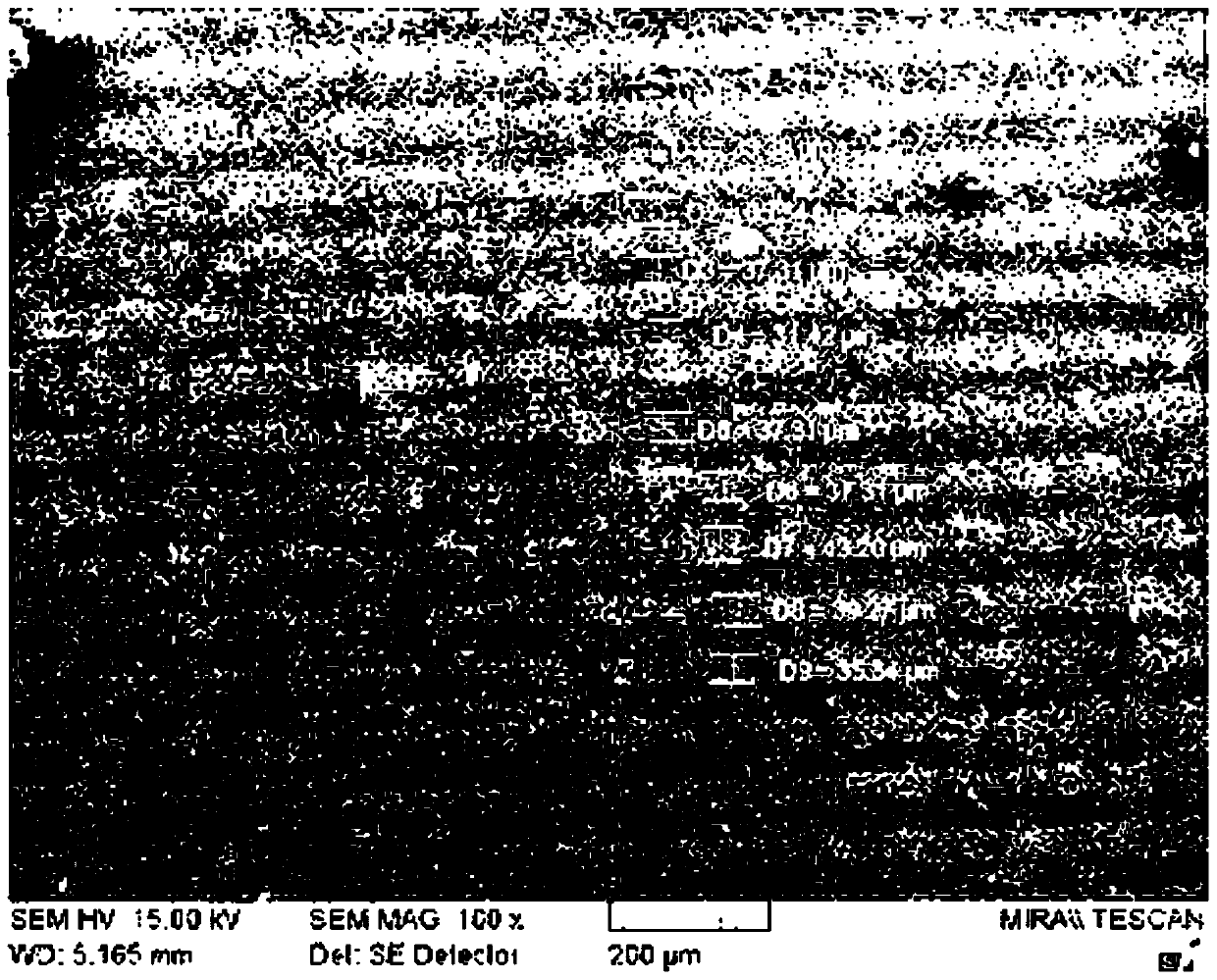
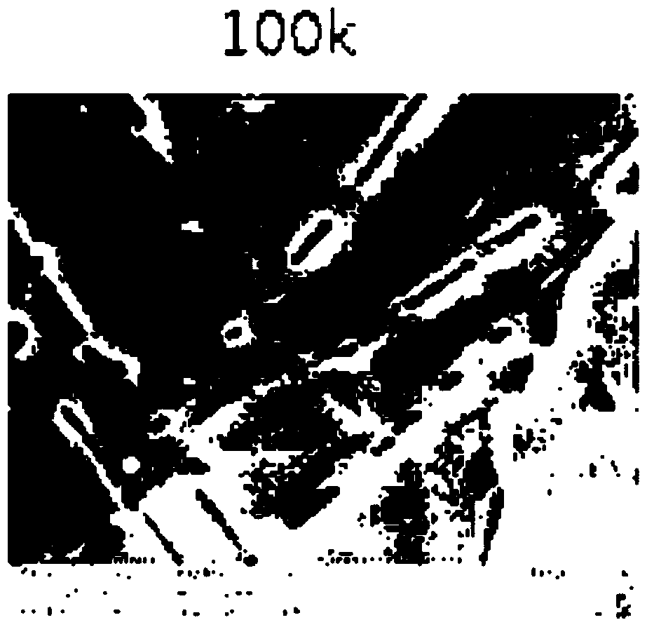
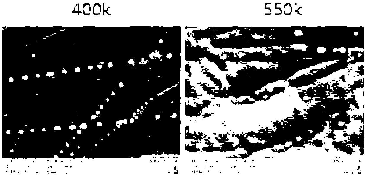
[0046] On the conductive electrode layer produced by the method of Production Example 1, a protective film was formed by the method of Production Example 2. In order to form a fine pattern on the surface of the electrode, an IR laser (manufacturer: EOTechnics) with a wavelength of 300-1064nm is directly irradiated onto the surface of the electrode layer with a frequency of 400kHz and a pulse width of 1-50ns to realize a fine pattern. (refer to image 3 )
PUM
| Property | Measurement | Unit |
|---|---|---|
| particle diameter | aaaaa | aaaaa |
| thickness | aaaaa | aaaaa |
Abstract
Description
Claims
Application Information
 - R&D
- Intellectual Property
- Life Sciences
- Materials
- Tech Scout
- Unparalleled Data Quality
- Higher Quality Content
- 60% Fewer Hallucinations
Browse by: Latest US Patents, China's latest patents, Technical Efficacy Thesaurus, Application Domain, Technology Topic, Popular Technical Reports.
© 2025 PatSnap. All rights reserved.Legal|Privacy policy|Modern Slavery Act Transparency Statement|Sitemap|About US| Contact US: help@patsnap.com