Component Substrate And Alignment Method

A technology of component substrates and substrates, which is applied in the direction of electrical components, electric solid devices, semiconductor devices, etc., can solve the problems of inconsistent anchoring force and poor alignment, and achieve the effect of improving poor alignment

Inactive Publication Date: 2015-01-07
AU OPTRONICS CORP
View PDF5 Cites 11 Cited by
  • Summary
  • Abstract
  • Description
  • Claims
  • Application Information

AI Technical Summary

Problems solved by technology

When using an alignment tool to carry out a contact alignment process on the alignment film, the amount of downward force of the alignment tool on the alignment film will be affected by the height difference between the test pad and the surrounding film layer, resulting in active components on the component substrate. The anchoring force of the alignment film near the junction of the region and the peripheral region and the center of the active region is inconsistent, that is, the problem of rubbing mura

Method used


Image

  • Component Substrate And Alignment Method
  • Component Substrate And Alignment Method
  • Component Substrate And Alignment Method

Examples


Embodiment Construction

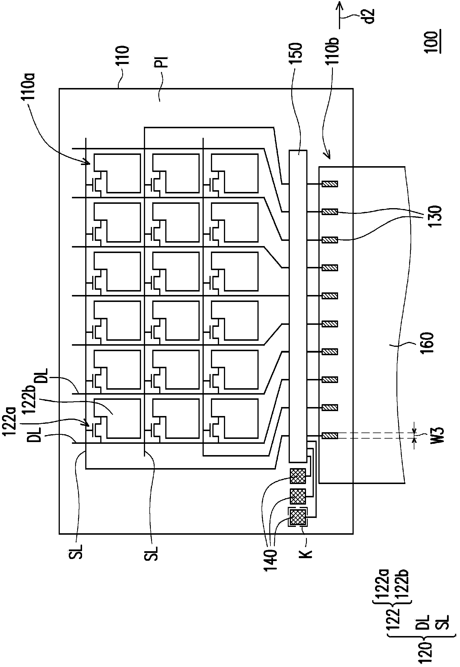
[0063] figure 1 It is a schematic top view of an element substrate according to an embodiment of the present invention. The device substrate 100 includes a substrate 110 , a pixel array 120 , a plurality of signal pads 130 and at least one test pad 140 . The substrate 110 has an active region 110a and a peripheral region 110b, the peripheral region 110b is connected to the active region 110a and surrounds the active region 110a. The pixel array 120 is located in the active region 110 a of the substrate 110 . A plurality of signal pads 130 are located in the peripheral region 110 b of the substrate 110 and are electrically connected to the pixel array 120 . At least one test pad 140 is located in the peripheral region 110 b of the substrate 110 and is electrically connected to the pixel array 120 . In this embodiment, the material of the substrate 110 can be glass, quartz, organic polymer, or opaque / reflective material (such as: conductive material, metal, wafer, ceramic, et...


PUM


Abstract

A component substrate includes a substrate having an active zone and a peripheral zone, a pixel array disposed in the active zone, a plurality of signal connecting pads disposed on the substrate and connected with the pixel array electrically and at least one testing connecting pad disposed in the peripheral zone and connected with the pixel array electrically. The testing connection pad includes a conducting layer disposed in the peripheral zone, an insulation layer covering the conducting layer and a contact pattern layer disposed on the insulation layer. The insulation layer has at least one contact opening and at least one groove. The conducting layer is exposed from the contact opening. The contact pattern layer is connected with the conducting layer electrically through the contact opening. A part of the contact pattern layer is disposed in the groove. Besides, the alignment method for the above component substrate is also disclosed. The alignment films on different areas on the substrate can have approximate anchoring forces, so that a problem of poor alignment in the prior art can be solved.

Description

technical field [0001] The present invention relates to a substrate and its alignment method, and in particular to an element substrate and its alignment method. Background technique [0002] The display panel includes an element substrate, an opposite substrate opposite to the element substrate, and a display medium arranged between the element substrate and the opposite substrate. Taking a liquid crystal display panel as an example, the display medium is a plurality of liquid crystal molecules. When the display panel is enabled, in order to enable the optical axis of the liquid crystal molecules to turn to the specified direction correctly and quickly, so as to provide the specified transmittance of the corresponding pixel, an alignment film is usually provided on the component substrate. Through the anchoring force provided by the alignment film, the optical axes of multiple liquid crystal molecules can be tilted in a specified direction when the display panel is not ena...

Claims


Application Information

Patent Timeline
Patent Type & Authority Applications(China)
IPC IPC(8): G02F1/1362G02F1/1337H01L27/12
CPCG02F1/133707H01L27/124
Inventor 王友志
Owner AU OPTRONICS CORP
Why Eureka
Try Eureka