
Rectilinear transmission type crystalline silicon solar cell printer with two sets of printing tables

A printing table and linear motion technology, which is applied to printing machines, rotary printing machines, screen printing machines, etc., can solve the problems of low production capacity, poor printing quality consistency, and low mechanical positioning accuracy

Inactive Publication Date: 2015-01-14
JIERUI LIGHT ENERGY SUZHOU
View PDF5 Cites 10 Cited by
  • Summary
  • Abstract
  • Description
  • Claims
  • Application Information

AI Technical Summary

Problems solved by technology

[0006] In order to solve the problems of low mechanical positioning accuracy and poor printing quality consistency of rotary table printing machines, and solve the problems of high debris and low production capacity of linear transmission printing equipment, and based on high-efficiency batteries for graphic recognition, high positioning accuracy and high-speed printing In order to meet the technical requirements, the present invention proposes a new method of loading and unloading and printing of silicon wafers, using two sets of printing tables driven by linear motion units to alternately complete the loading, unloading and printing of silicon wafers

Method used


Image

  • Rectilinear transmission type crystalline silicon solar cell printer with two sets of printing tables
  • Rectilinear transmission type crystalline silicon solar cell printer with two sets of printing tables
  • Rectilinear transmission type crystalline silicon solar cell printer with two sets of printing tables

Examples


Embodiment Construction

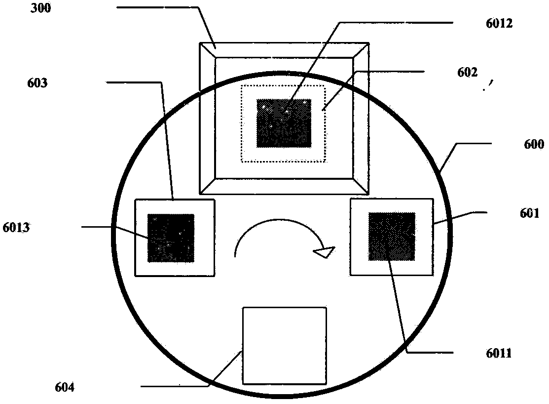
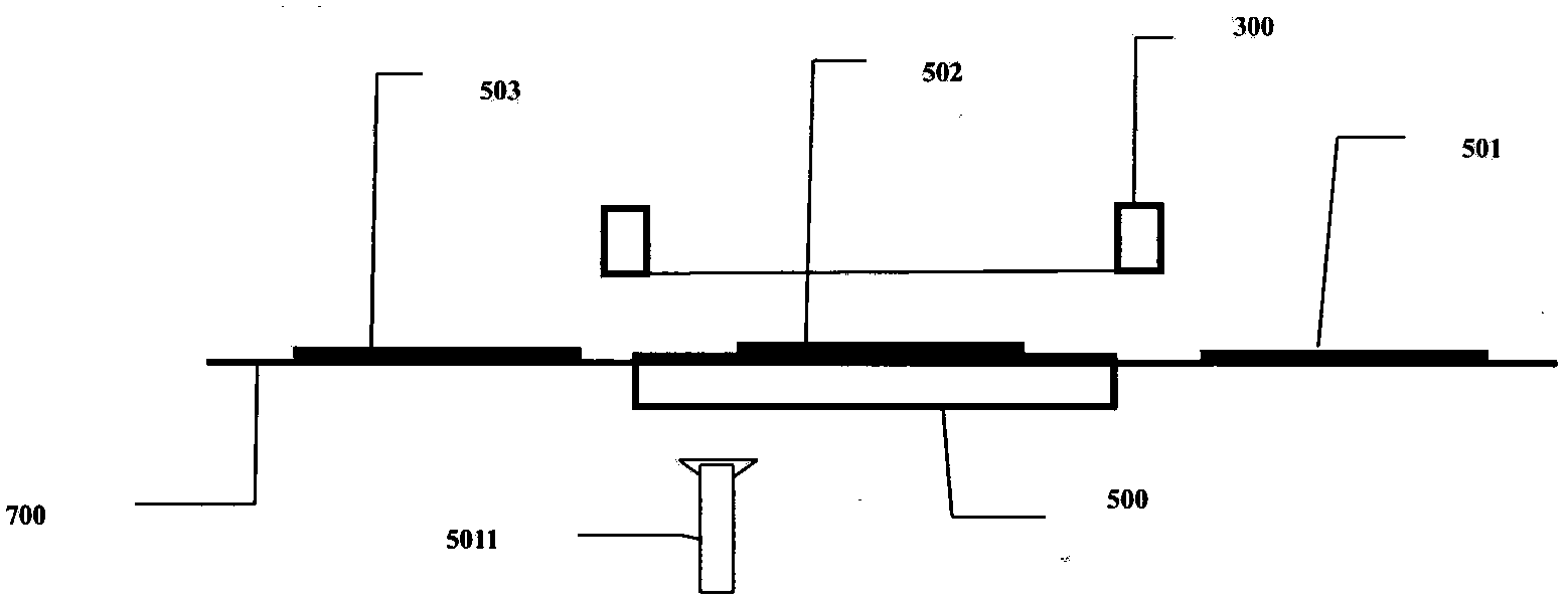
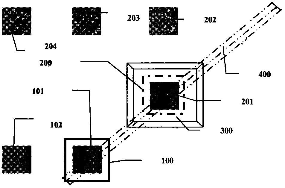
[0012] The silicon wafer loading and unloading and printing methods proposed by the present invention are as follows: image 3 As shown, after the silicon wafer 101 is transferred to the printing table 100, the vacuum system on the printing table 100 adsorbs and fixes the silicon wafer 101, and the camera system located above the printing table 100 detects the shape of the silicon wafer 101, and according to the cell technology The position information of the silicon wafer 101 or the position information of the existing process patterns on the silicon wafer 101 (such as the front silver gate line printed for the first time, or the selective re-expansion area, etc.) is collected. At the same time, the printing table 200 is in the printing station directly below the printing screen 300 , and the printing equipment completes the printing of the silicon wafer 201 on the printing table 200 . After the printing is completed, the printing table 200 will leave the printing station wit...


PUM


Abstract

The invention provides a silicon wafer feeding and discharging and printing method adopting two sets of printing tables and applied to crystalline silicon solar cell electrode printing production equipment, and relates to a rectilinear transmission type crystalline silicon solar cell printer with two sets of printing tables. Through the method for alternatively and simultaneously completing silicon wafer feeding and discharging and printing with the two sets of printing tables, printing equipment achieves higher productivity within unit time; rectilinear motion units are adopted to translate the printing tables between a silicon wafer feeding and discharging station and a printing station, and accurate positioned printing of cells is realized by virtue of single-degree-of-freedom high repeatability positioning accuracy; by the same set of camera system, pre-printing and post-printing data analysis is performed on the same silicon wafer on the same feeding and discharging station, and various technological functions including printing accuracy, broken gate detection, screen technique life monitoring, secondary printing screen matching monitoring are realized.

Description

technical field [0001] The silicon wafer transfer positioning method proposed by the invention is applied in the field of crystalline silicon solar cell electrode printing and production, and is suitable for high-speed mass production printing of high-efficiency crystalline silicon solar cell electrodes with high requirements on printing accuracy and printing quality. Background technique [0002] At present, there are two types of conventional printing machines for crystalline silicon solar cells. One is a printing machine structure that uses a rotary table to realize loading and unloading and printing of silicon wafers; the other is a linear transmission structure that uses a belt to transfer silicon wafers to the printing table for printing. . [0003] Printing equipment using a rotating table, such as figure 1 As shown, the loading of the silicon wafer 6013 and the position collection of the silicon wafer can be completed on the table 603 at the same time, the printing ...

Claims


Application Information

Patent Timeline
IPC IPC(8): B41F15/08H01L31/18
CPCY02P70/50
Inventor 于国丰杨杰
Owner JIERUI LIGHT ENERGY SUZHOU
Learn More