Solid state imaging apparatus, production method thereof and electronic device

A technology of solid-state imaging device and insulating structure, applied in semiconductor/solid-state device manufacturing, radiation control device, television, etc., can solve problems such as deterioration of flash, and achieve the effect of reducing flash components

Active Publication Date: 2015-01-14
SONY CORP
View PDF9 Cites 3 Cited by
  • Summary
  • Abstract
  • Description
  • Claims
  • Application Information

AI Technical Summary

Problems solved by technology

Therefore, the incident light is reflected by the guard ring, so the flash becomes bad

Method used


Image

  • Solid state imaging apparatus, production method thereof and electronic device
  • Solid state imaging apparatus, production method thereof and electronic device
  • Solid state imaging apparatus, production method thereof and electronic device

Examples


no. 1 example

[0048] 2. First Embodiment (Configuration Example of Laminated Back-illuminated Solid-State Imaging Device)

no. 2 example

[0049] 3. Second Embodiment (Configuration Example of Non-Laminated Back-illuminated Solid-State Imaging Device)

[0050] 4. The third embodiment (retaining ring structure with arcuate shape)

[0051] 5. Fourth Embodiment (Trench structure between pixels with arcuate shape)

[0052] 6. Application of electronic equipment

[0053]

[0054]

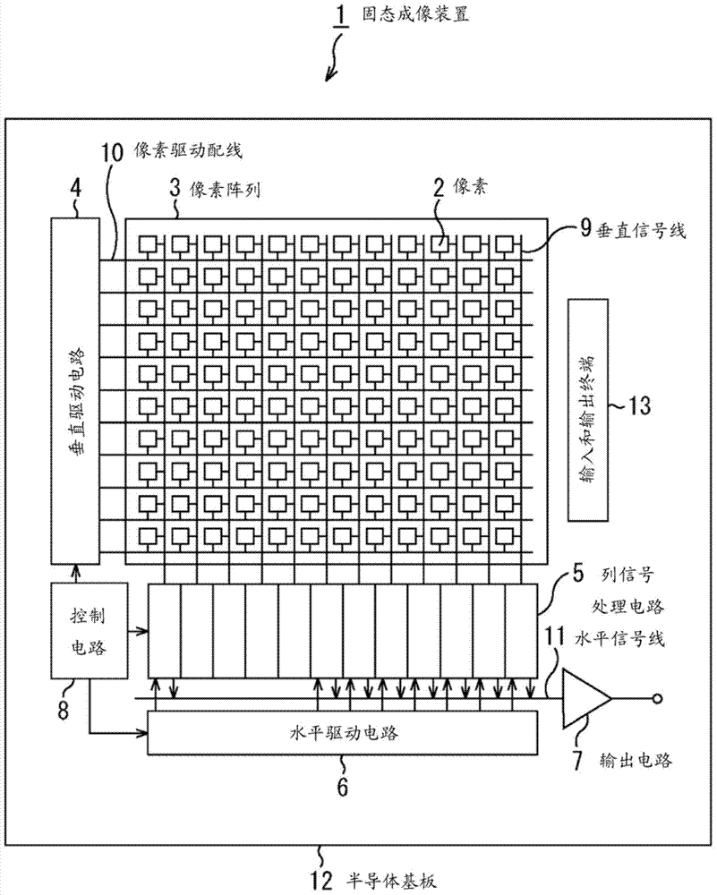
[0055] figure 1 A schematic configuration of a solid-state imaging device according to an embodiment of the present disclosure is shown.

[0056] figure 1 The illustrated solid-state imaging device 1 includes a semiconductor substrate 12 using silicon (Si) as a semiconductor, a pixel array 3 in which pixels 2 are arranged in a two-dimensional array, and peripheral circuits. The peripheral circuit includes a vertical drive circuit 4 , a column signal processing circuit 5 , a horizontal drive circuit 6 , an output circuit 7 and a control circuit 8 .

[0057] Each pixel 2 includes a photodiode as a photoelectric conversion element and...

no. 3 example

[0205]

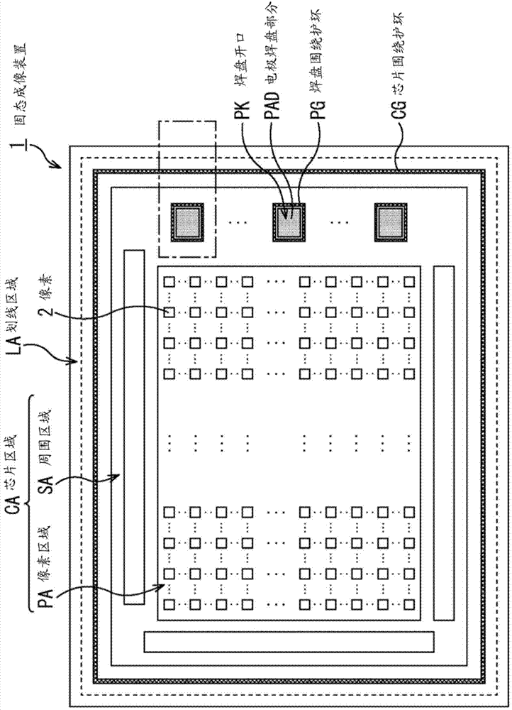
[0206] In the above-described embodiments, each of the pad surrounding guard ring PG and the chip surrounding guard ring CG has a forward tapered shape in which the top diameter on the light incident surface side is larger than the bottom diameter on the bottom. Other structures of the pad surrounding guard ring PG and the chip surrounding guard ring CG will be described below.

[0207] The pad surrounding guard ring PG and the chip surrounding guard ring CG may be formed by forming an opening 202 having a high aspect ratio to a semiconductor substrate 201 by a dry etching process and spin-coating a coating material 203 by a spin coating method to fill the opening 202 with the coating material 203. ,Such as Figure 21 shown.

[0208] However, depending on the shape of the opening 202, the coating material 203 on the upper part of the opening 202 may spill due to the centrifugal force of the rotation, as Figure 21 shown. Once the coating material 203 spills out a...


PUM


Abstract

A solid state imaging apparatus includes an insulation structure formed of an insulation substance penetrating through at least a silicon layer at a light receiving surface side, the insulation structure having a forward tapered shape where a top diameter at an upper portion of the light receiving surface side of the silicon layer is greater than a bottom diameter at a bottom portion of the silicon layer. Also, there are provided a method of producing the solid state imaging apparatus and an electronic device including the solid state imaging apparatus.

Description

technical field [0001] The present disclosure relates to a solid-state imaging device, a manufacturing method thereof, and electronic equipment, particularly a solid-state imaging device capable of reducing flare components, a manufacturing method thereof, and electronic equipment. Background technique [0002] A method of manufacturing a semiconductor chip includes forming a plurality of semiconductor chips on a wafer, and dicing the semiconductor chips along a scribe area using a blade to separate the semiconductor chips. In this method, possible chipping by cutting should be prevented. [0003] When wire-bonding the electrode pads in the semiconductor chip, or when probing the electrode pads during inspection, no leakage or damage should occur even if the side walls come into contact with the bonding wires or probes. [0004] In order to prevent possible chipping by cutting with a blade or leakage or damage during wire bonding or probing, solid-state imaging devices havi...

Claims


Application Information

Patent Timeline
Patent Type & Authority Applications(China)
IPC IPC(8): H01L27/146
CPCH01L27/14643H01L27/14683H01L27/14601H01L27/14627H01L27/14629H01L27/1463H01L27/14634H01L27/14636H01L27/1464H01L27/1469H01L27/14623H01L27/1462H01L27/14621H01L27/14632H01L27/14645H01L27/14685H01L27/14687H01L21/7682H01L21/76898H04N25/616H04N25/772H01L31/022416
Inventor 水田恭平大地朋和千叶洋平
Owner SONY CORP
Why Eureka
Try Eureka