Backlight source and display device

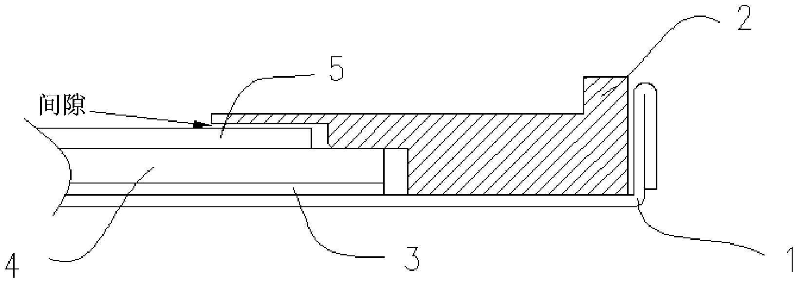
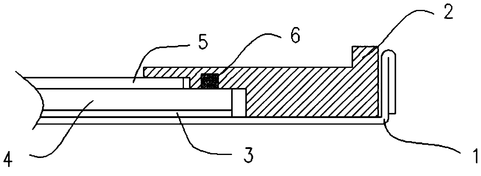
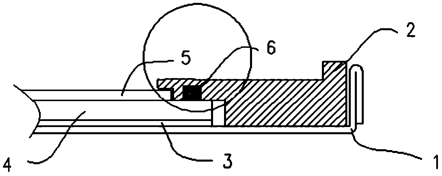
A technology of backlight and light guide plate, which is applied in the direction of light guide, optics, optical components, etc., and can solve problems that affect the development process of backlight, chipping of optical film 5, difficulty in passing reliability test, etc.

Active Publication Date: 2015-01-21
HEFEI BOE OPTOELECTRONICS TECH +1
View PDF5 Cites 10 Cited by
  • Summary
  • Abstract
  • Description
  • Claims
  • Application Information

AI Technical Summary

Problems solved by technology

figure 1 It shows a schematic cross-sectional view of a backlight source in the prior art. Modules such as a frame 2, a bottom reflector 3, a light guide plate 4, and an optical film 5 are arranged in a backplane 1. During the development process of a backlight source, the frame 2 and the optical film The size of the gap (at the arrow) between 5 is difficult to grasp
When the current backlight is subjected to vibration tests, if the gap between the optical film 5 and the frame 2 is too large, the optical film 5 will move on the surface of the light guide plate 4 and cause physical friction, causing the backlight to be scratched badly. Or the optical film 5 will be chipped and cause foreign matter failure; if the gap is too small, the expansion of the light guide plate 4 and the optical film 5 will further squeeze the gap during the high temperature and high humidity test of the backlight, which will cause the backlight to produce film drums. Bad (Sheet Wrinkle), which makes it difficult to pass the reliability test during the development process and affects the development process of the backlight

Method used


Image

  • Backlight source and display device
  • Backlight source and display device
  • Backlight source and display device

Examples


Embodiment Construction

[0022] In order to more clearly understand the above objects, features and advantages of the present invention, the present invention will be further described in detail below in conjunction with the accompanying drawings and specific embodiments. It should be noted that, in the case of no conflict, the embodiments of the present application and the features in the embodiments can be combined with each other.

[0023] In the present invention, the terms "first" and "second" are used for descriptive purposes only, and should not be understood as indicating or implying relative importance. The term "plurality" means two or more, unless otherwise clearly defined. In addition, it will be understood that when an element or layer is referred to as being "on" another element or layer, it can be directly on the other element or intervening layers may be present. When a layer is "under" it can be directly under other elements, or one or more intervening layers or elements may be prese...


PUM


Abstract

The invention relates to a backlight source and a display device. The backlight source comprises a frame, an optical film, a light guide plate and an embedded block. The coefficient of volume expansion of the embedded block is higher than that of the frame. A first transverse protrusion is formed on one side, close to the light guide plate, of the frame, and the lower surface of the first transverse protrusion is in press fit with the light guide plate. The embedded block is arranged in a groove formed in the lower surface of the first transverse protrusion. A second transverse protrusion is formed on the upper portion of the side, close to the optical film, of the first transverse protrusion, and the lower surface of the second transverse protrusion is in press fit with the optical film. According to the technical scheme, in vibration test of the backlight source, chippings of the optical film or scratch of the backlight source can be avoided; in high-temperature high-humidity test, over-compression between the optical film and the second transverse protrusion can be avoided so as to prevent bulge of the optical film.

Description

technical field [0001] The present invention relates to the field of display technology, in particular, to a backlight source and a display device. Background technique [0002] A liquid crystal display (Liquid Crystal Display) mainly includes a liquid crystal panel and a backlight. Backlight can be mainly divided into LED (Light Emitting Diode, LED for short) backlight and CCFL (Cold Cathode Fluorescent Lamp, CCFL for short) backlight according to the type of light source; it can be divided into Mobile, Tablet, Notebook, Monitor, TV, etc. In recent years, LED backlight has become the best choice in the field of liquid crystal display due to its excellent optical effect and thinning trend of display devices. [0003] Backlight needs to go through a series of tests during the development process, such as vibration test, thermal shock test, high temperature and high humidity test, drop test and so on. figure 1 It shows a schematic cross-sectional view of a backlight source ...

Claims


Application Information

Patent Timeline
Patent Type & Authority Applications(China)
IPC IPC(8): G02F1/13357G02F1/1333G02F1/13
CPCG02B6/0065G02B6/0055G02B6/0088G02F1/133608G02F1/133308G02F1/133603
Inventor 陈守年陈东
Owner HEFEI BOE OPTOELECTRONICS TECH
Why Eureka
Try Eureka