LDMOS device and manufacture method thereof

A device and metal technology, applied in the field of LDMOS devices and its manufacturing process, can solve the problems of high thermal budget and affecting the shape of other junction regions, etc., and achieve the effects of low thermal budget, low on-resistance, and high breakdown voltage

Inactive Publication Date: 2015-01-21
CHENGDU MONOLITHIC POWER SYST
View PDF4 Cites 11 Cited by
  • Summary
  • Abstract
  • Description
  • Claims
  • Application Information

AI Technical Summary

Problems solved by technology

However, this solution requires a higher thermal budget and thus affects the shape of other junction regions

Method used


Image

  • LDMOS device and manufacture method thereof
  • LDMOS device and manufacture method thereof
  • LDMOS device and manufacture method thereof

Examples


Embodiment Construction

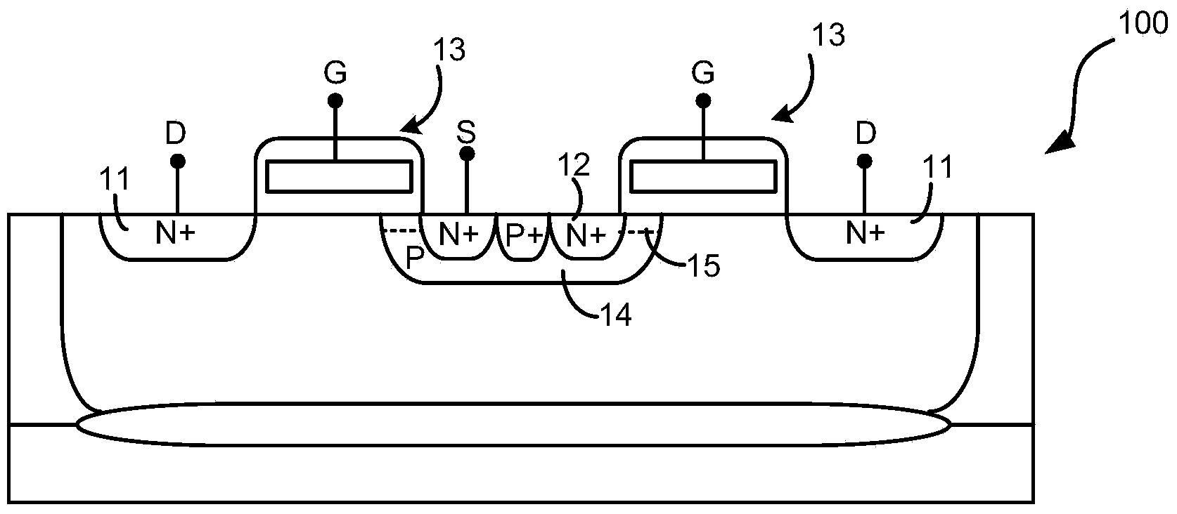
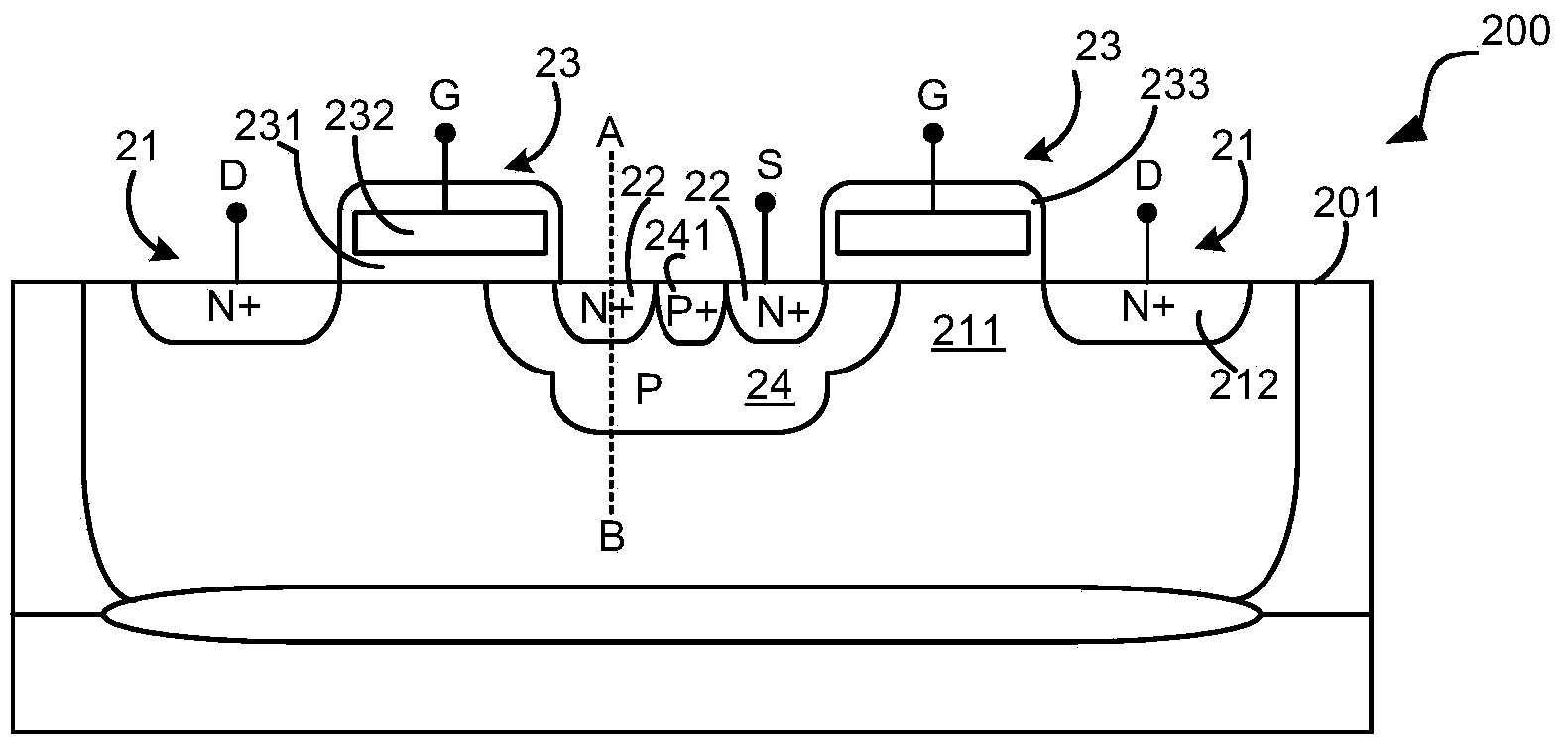
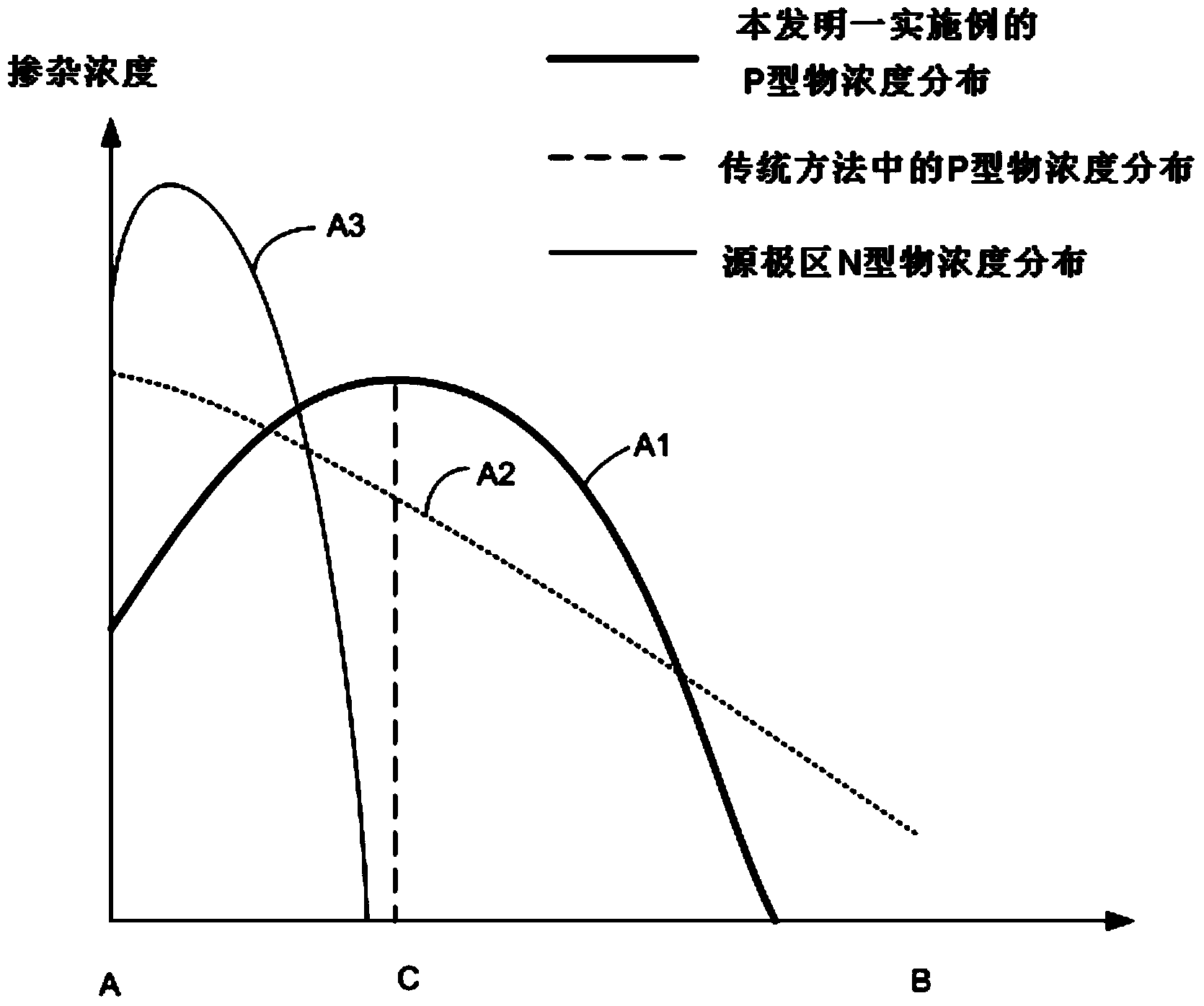
[0018] Specific embodiments of the present invention will be described in detail below, and it should be noted that the embodiments described here are only for illustration, not for limiting the present invention. In the following detailed description of the invention, numerous details are set forth in order to better understand the invention. However, it will be understood by those skilled in the art that the present invention may be practiced without these specific details. In order to clearly illustrate the present invention, detailed descriptions of some specific structures and functions are simplified herein. In addition, similar structures and functions that have been described in detail in some embodiments will not be repeated in other embodiments. Although terms of the present invention have been described in conjunction with specific exemplary embodiments, these terms should not be construed as being limited to the exemplary embodiments set forth herein. Meanwhile, ...


PUM


Abstract

The invention discloses an LDMOS device and a manufacture method thereof. The manufacture method of the LDMOS device comprises the steps of fabricating a gate region of the LDMOS device on a semiconductor substrate, employing a mask to inject a first doping matter into the semiconductor substrate obliquely at a certain angle and employing the same masking to inject the first doping matter into the semiconductor substrate vertically, wherein the region formed by inclined injection and the region formed by vertical injection are jointly used for forming a body region of the LDMOS device; and fabricating a source electrode region and a drainage electrode contact region of the LDMOS device, wherein the source electrode region and the drainage electrode contact region adopt second doping different from first doping. The method and device are advantaged by low thermal budget, low on-resistance, and high breakdown voltage.

Description

technical field [0001] The invention relates to a semiconductor device, in particular to an LDMOS device and a manufacturing process thereof. Background technique [0002] Compared with other types of transistors, lateral metal-oxide-semiconductor field-effect transistors (LDMOS) have high breakdown voltage and good thermal characteristics, and thus are widely used. Such as figure 1 As shown, an LDMOS device 100 includes a drain 11 , a source 12 , a gate 13 and a body region 14 . When a voltage is applied to the gate 13, the channel region 15 below the gate 13 is inverted from P-type to N-type, a current path is formed between the drain 11 and the source 12, and the LDMOS is turned on. [0003] High breakdown voltage and low on-resistance are two important parameters expected from LDMOS devices. In order to make LDMOS devices with low on-resistance and small cell size, one solution is to use short channels. However, the existing short-channel process results in lower bre...

Claims


Application Information

Patent Timeline
Patent Type & Authority Applications(China)
IPC IPC(8): H01L29/78H01L21/336
CPCH01L21/26586H01L29/086H01L29/0878H01L29/1095H01L29/66681H01L29/7816
Inventor 郑志星乔伊·迈克格雷格吉扬永
Owner CHENGDU MONOLITHIC POWER SYST
Why Eureka
Try Eureka