GeSn infrared detector with strain source
An infrared detector and array technology, which is applied in the field of infrared detection, can solve the problems of material quality and thermal stability variation, difficulty in wide-range bandgap adjustment, etc., and achieve the effect of adjustable energy band
- Summary
- Abstract
- Description
- Claims
- Application Information
AI Technical Summary
Problems solved by technology
Method used
Image
Examples
Embodiment Construction
[0029] In order to understand the technical essence of the present invention more clearly, the structure and process realization of the present invention are described in detail below in conjunction with the accompanying drawings and embodiments:
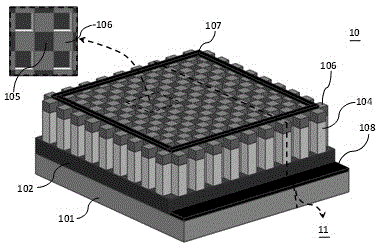
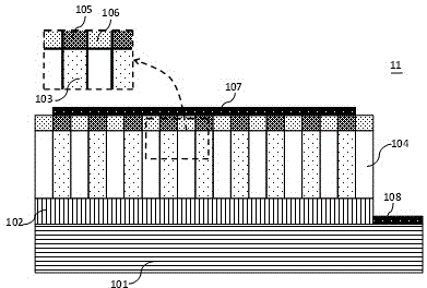
[0030] Among them, the light absorbing array is made of single crystal GeSn material, the strain source array is made of single crystal SiGe material distributed around the light absorbing unit, the GeSn metal contact array and the SiGe metal contact array are respectively located on the light absorbing array and the strain source array, the first electrode Surrounding the top of the metal contact array, the second electrode is on the substrate.
[0031] see figure 1 and figure 2 GeSn infrared detector with strain source shown, which has n + Si substrate 101, relaxation layer 102, light absorption array 103, strain source array 104, GeSn metal contact array 105, SiGe metal contact array 106, first electrode 107, second electrode...
PUM
 Abstract
Description
Claims
Application Information


