

Semiconductor device and fabrication method
a technology of semiconductors and dielectric layers, applied in the direction of semiconductor devices, basic electric elements, electrical equipment, etc., can solve the problems of more defects in the structure of conventional mos field effect transistors (fets) cannot meet the requirements of device performance, and the electrical properties of the high-k gate dielectric layer can be affected
- Summary
- Abstract
- Description
- Claims
- Application Information
AI Technical Summary
Benefits of technology
Problems solved by technology
Method used
Image

Examples
Embodiment Construction
[0012]Reference will now be made in detail to exemplary embodiments of the disclosure, which are illustrated in the accompanying drawings. Wherever possible, the same reference numbers will be used throughout the drawings to refer to the same or like parts.
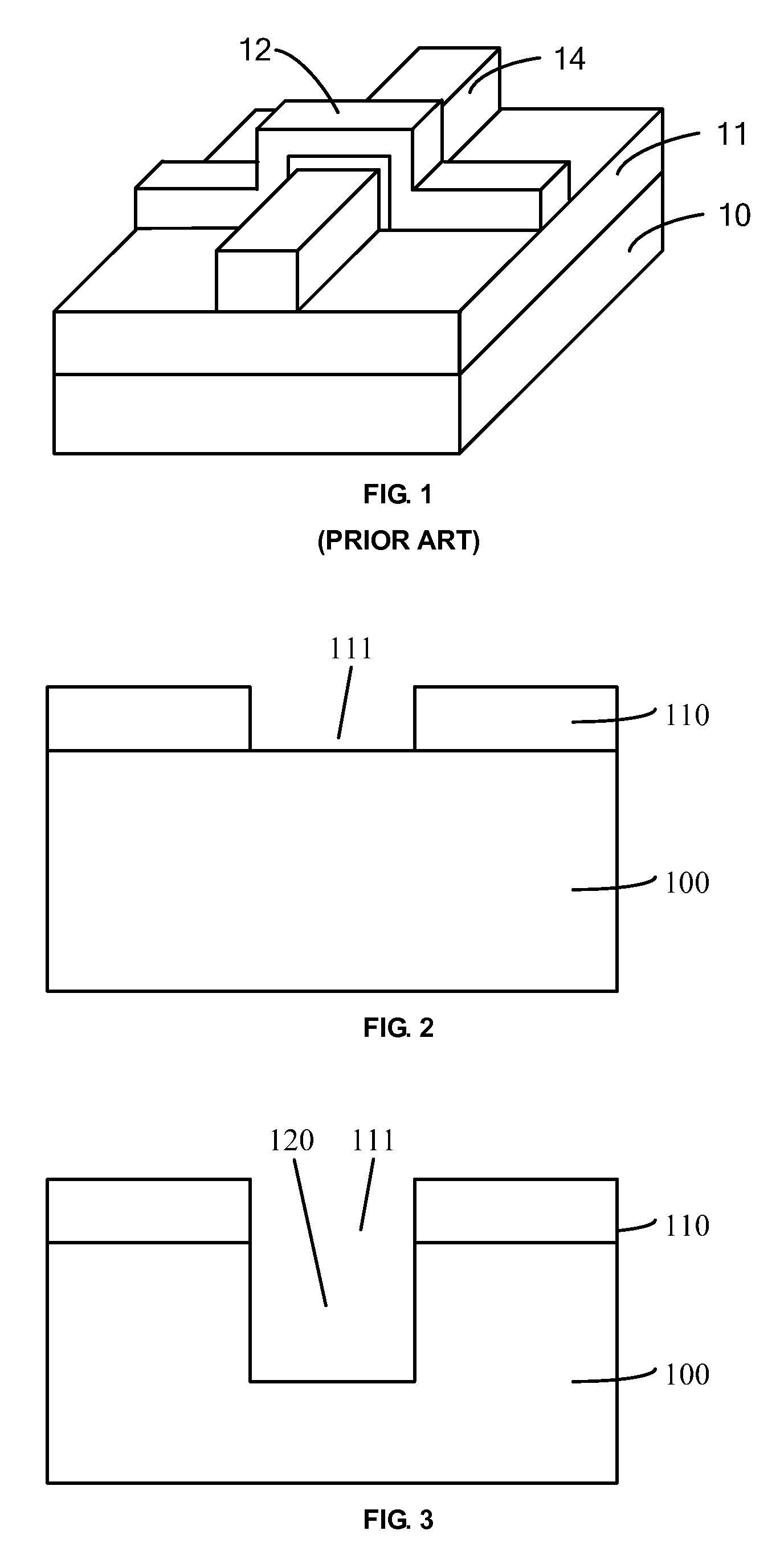
[0013]To improve the device performance of fin FET, carrier mobility in a channel region may be enhanced. However, conventional methods for enhancing carrier mobility in the channel region can affect the electrical properties of a high-k gate dielectric layer of the fin FET.
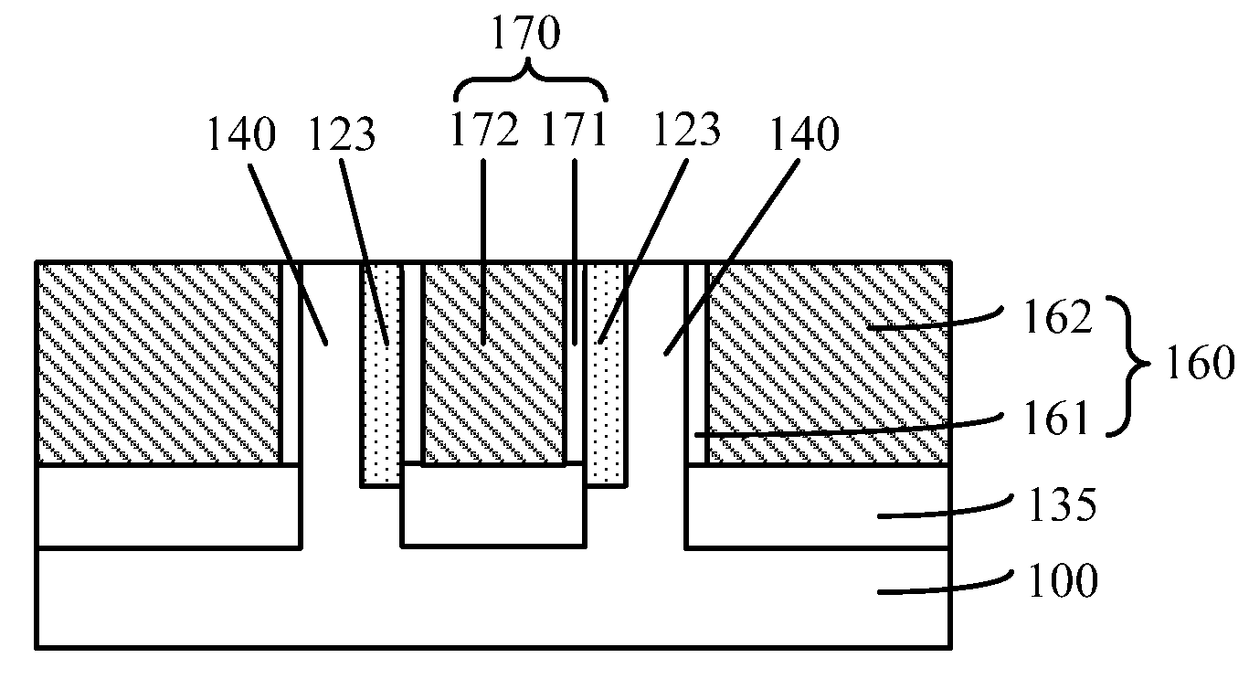
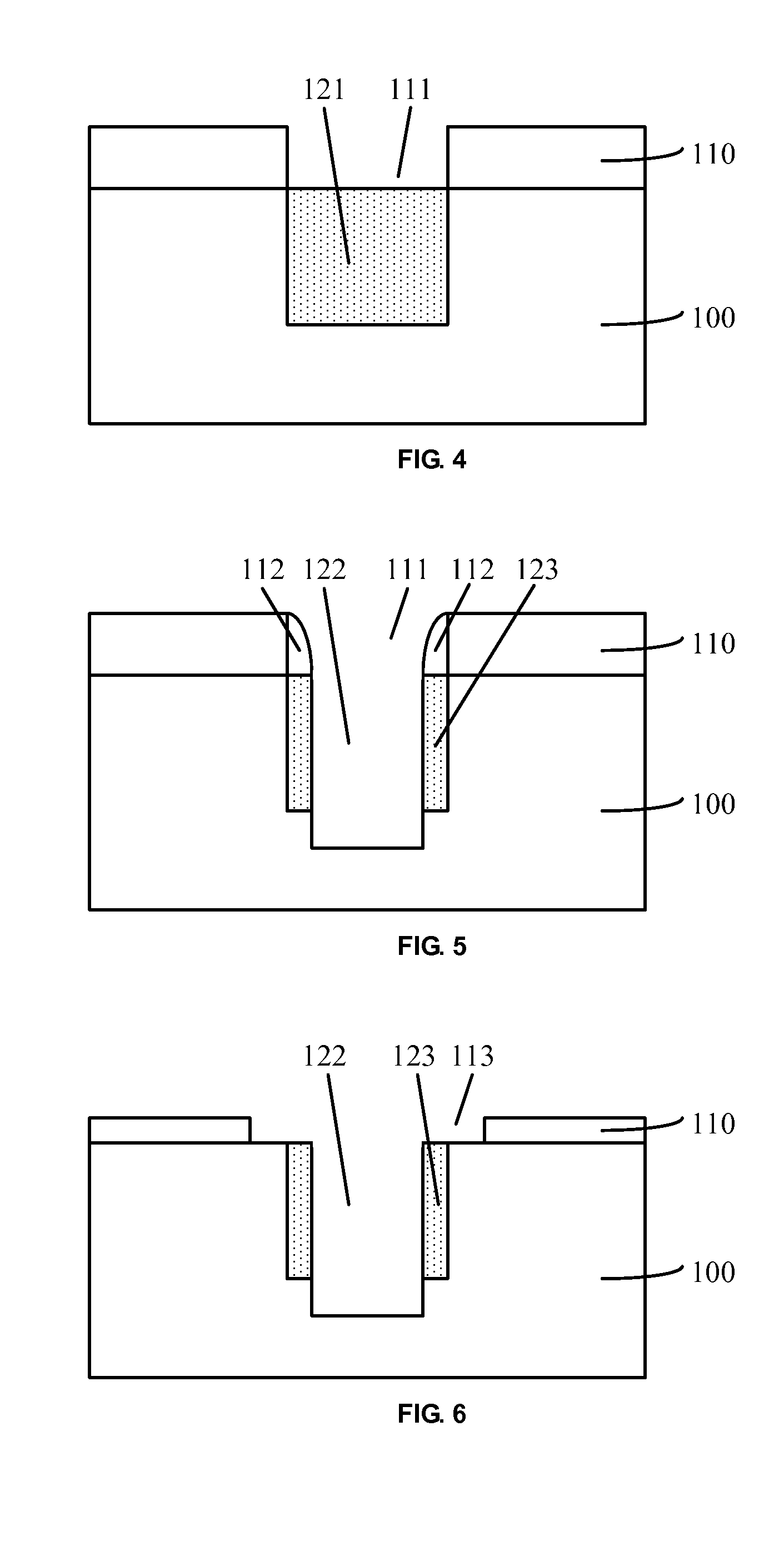
[0014]Disclosed herein includes a semiconductor structure and a fabrication method for making the same. The semiconductor structure includes a semiconductor substrate, a fin structure on the semiconductor structure, a main gate structure on one sidewall of the fin structure, a stress material layer on the other sidewall of the fin structure, and a back gate structure on the sidewalls of the stress material layer located between the fin structure and the back ga...
PUM
| Property | Measurement | Unit |
|---|---|---|
| depth | aaaaa | aaaaa |
| width | aaaaa | aaaaa |
| width | aaaaa | aaaaa |
Abstract
Description
Claims
Application Information