
Camera soft and hard combination board manufacturing method

A technology of soft-rigid combination board and production method, which is applied in the direction of printed circuit manufacturing, electrical components, and printed circuit assembly of electrical components, which can solve the problems of large thickness and difficulty in application, and achieve the effect of reducing thickness

Active Publication Date: 2015-01-21
台山市精诚达电路有限公司
View PDF4 Cites 8 Cited by
  • Summary
  • Abstract
  • Description
  • Claims
  • Application Information

AI Technical Summary

Problems solved by technology

[0004] The four-layer soft-rigid combination board for the camera produced by the existing technology generally has a total thickness of about 0.40mm---0.45mm, and rarely can achieve a total thickness of 0.30mm. The reason is that the current materials are directly laminated and laminated, and the thickness is natural Larger, it is difficult to apply to some environments that have special requirements for thickness, such as the flexible and rigid combination board of the camera of the mobile terminal

Method used


Image

  • Camera soft and hard combination board manufacturing method
  • Camera soft and hard combination board manufacturing method
  • Camera soft and hard combination board manufacturing method

Examples


Embodiment Construction

[0027] In order to describe the technical content, achieved goals and effects of the present invention in detail, the following descriptions will be made in conjunction with the embodiments and accompanying drawings.

[0028] Glossary:

[0029] High TP copper plating solution: when FPC or PCB is electroplated with this copper plating solution, the ratio of the copper thickness obtained by electroplating the via hole to the copper thickness obtained by electroplating the board surface is greater than 1.5:1, where TP refers to electroplated copper The through power of the circuit board is the ratio of the copper plating of the circuit board, the thickness of the hole copper to the thickness of the surface copper. The higher the TP, the thinner the surface copper when the hole copper is the same;

[0030] Copper reduction treatment by micro-etching method: Copper reduction treatment by micro-etching method refers to copper reduction treatment with a micro-etching solution prepar...


PUM

PropertyMeasurementUnit
Thicknessaaaaaaaaaa
Thicknessaaaaaaaaaa
Thicknessaaaaaaaaaa

Abstract

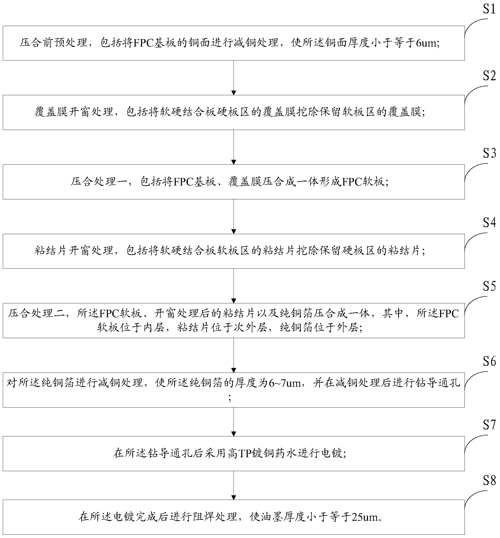
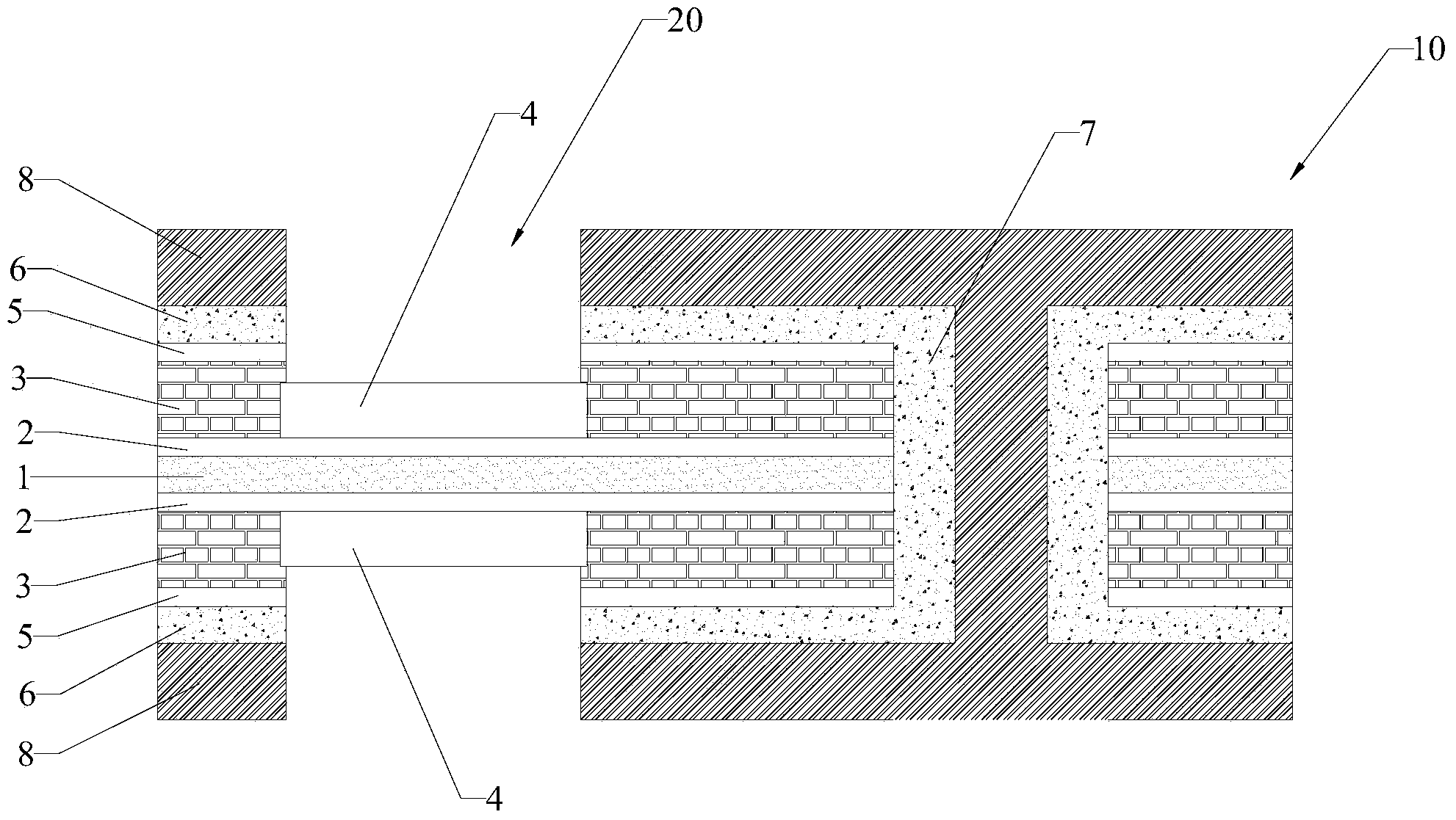
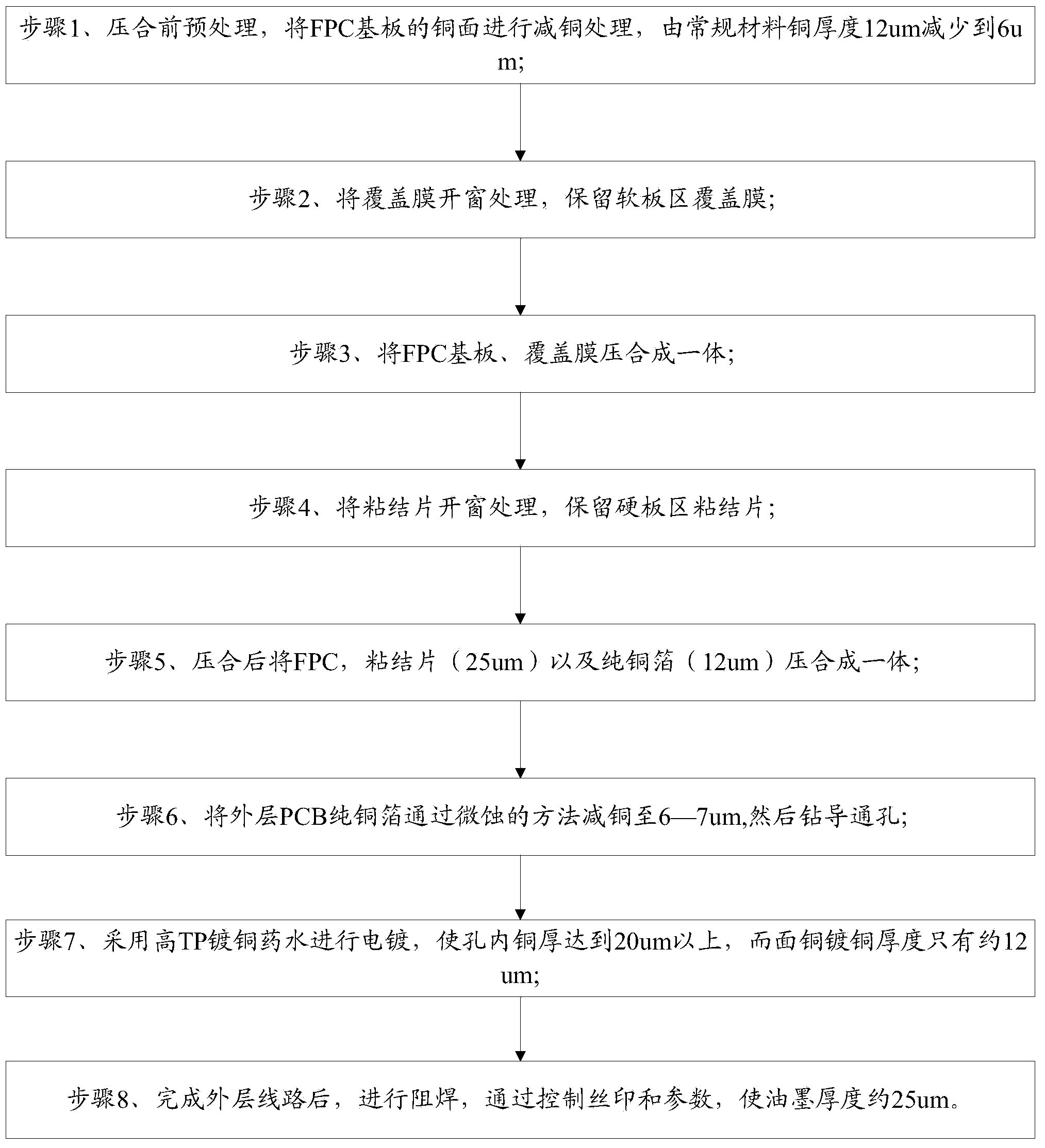
The invention discloses a camera soft and hard combination board manufacturing method. The method includes the steps that preprocessing before press fit is performed, wherein copper reduction processing is performed on the copper surface of an FPC substrate; covering film windowing is performed, wherein a covering film on a hard board area is removed in an excavation mode and a covering film in a soft board area is reserved; the FPC substrate and the covering film are integrated through press fit to form a soft FPC board; bonding sheet windowing is performed, wherein bonding sheets in the soft board area of a soft and hard combination board are moved in an excavation mode and bonding sheets in the hard board area of the soft and hard combination board are reserved; second press fit processing is performed, wherein the soft FPC board, the bonding sheets subjected to windowing and pure copper foil are integrated through press fit; copper reduction processing is performed on the pure copper foil, the thickness of the pure copper foil is made to range from 6 microns to 7 microns, and through holes are drilled after copper reduction processing; after the through holes are drilled, a high-TP copper-plating solution is adopted for electroplating; after the electroplating, solder resisting is performed, and the thickness of printing ink is made to be smaller than or equal to 25 microns. Through the method, the thickness of the soft and hard combination board can be effectively reduced.

Description

technical field [0001] The invention relates to the field of circuit board manufacture, in particular to a method for manufacturing a camera-flex-hard combination board. Background technique [0002] Rigid-flex board is a circuit board with FPC characteristics and PCB characteristics formed by combining flexible circuit boards and rigid circuit boards through lamination and other processes according to relevant process requirements. It can be used in some products with special requirements. It has both a certain flexible area and a certain rigid area. It is of great help to save the internal space of the product, reduce the volume of the finished product, and improve the performance of the product. [0003] The production process of the soft-rigid board is as follows. First, the electronic engineer draws the circuit and shape of the flexible board according to the requirements, and then sends it to the factory that can produce the soft-hard board. After the CAM engineer proc...

Claims


Application Information

Patent Timeline
IPC IPC(8): H05K3/00H05K3/36
Inventor 苏章泗韩秀川刘振华
Owner 台山市精诚达电路有限公司
Learn More