Method for forming self-alignment metal silicide

A technology of metal silicide and metal silicide layer, applied in electrical components, semiconductor/solid-state device manufacturing, semiconductor devices, etc., can solve problems such as poor NBTI performance and negative threshold voltage drift, so as to improve NBTI performance and reduce defects , Repair and Defect Effects

Inactive Publication Date: 2015-01-28
SHANGHAI HUALI MICROELECTRONICS CORP
View PDF4 Cites 2 Cited by
  • Summary
  • Abstract
  • Description
  • Claims
  • Application Information

AI Technical Summary

Problems solved by technology

In the existing manufacturing process, there are a large number of hole defects and Si-H bonds at the interface between the metal silicide and the silicon substrate. During the NBTI test, the Si-H bonds are thermally excited and broken to form Si dangling bonds. Combined with hydrogen and released in the form of hydrogen, further forming hole defects, causing a negative shift in the threshold voltage, making the NBTI performance of the device poor

Method used


Image

  • Method for forming self-alignment metal silicide
  • Method for forming self-alignment metal silicide
  • Method for forming self-alignment metal silicide

Examples


Embodiment Construction

[0034] Embodiments of the present invention use the existing commonly used Ni as the material for forming metal silicides, and are based on a two-step annealing process, combining Figure 4 to Figure 5 , to explain the improvement of the technical solution of the present invention in detail, but the technical solution of the present invention is not limited thereto.

[0035] The method for forming the salicide of this embodiment includes the following steps:

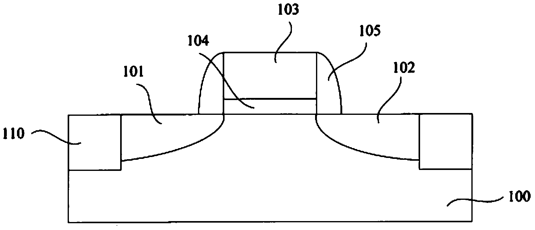
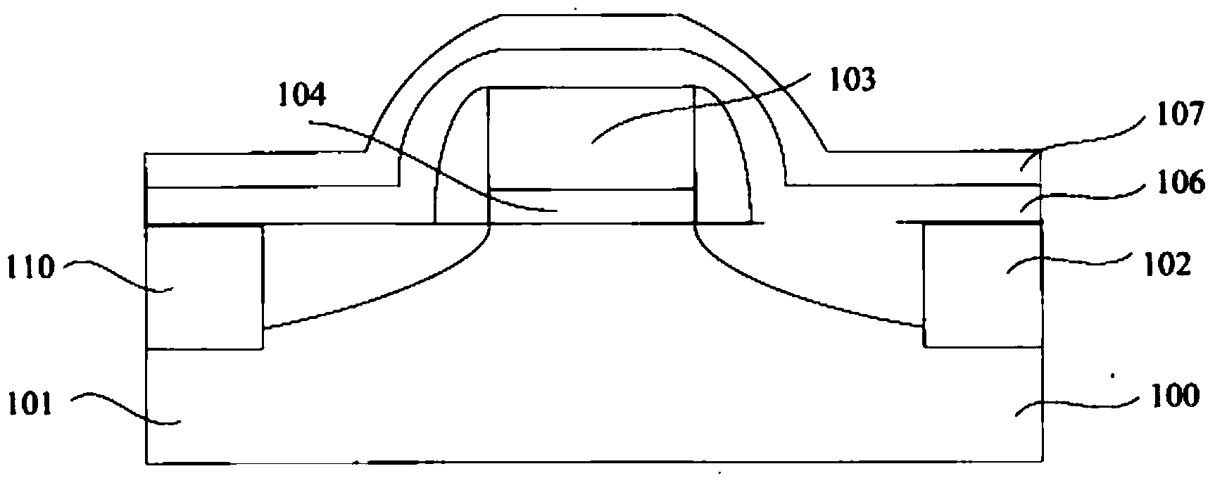
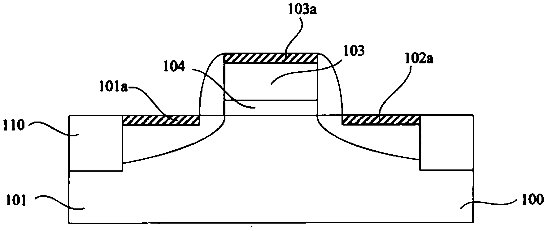
[0036] Step 1, such as Figure 4As shown, a semiconductor substrate 11 is provided. The surface of the substrate 11 has a silicon region, and the silicon region includes a gate 12 of a MOS transistor and a source region 13 and a drain region 14 formed in the substrate 11 on both sides of the gate 12 . The gate 12 includes a gate dielectric layer 121 , a gate electrode layer 122 , and spacers 123 formed on both sides of the gate dielectric layer and the gate electrode layer.

[0037] Before depositing the metal layer, t...


PUM


Abstract

The invention discloses a method for forming a self-alignment metal silicide. The two times of annealing technologies are adopted, hydrogen isotope gas is introduced in the first time of annealing technology, the hydrogen isotope gas is used for reacting with trace oxygen in the atmosphere to eliminate the oxygen, metal layers such as Ni are prevented from being oxidized, and therefore surface defects (such as a pyramid shape) of the metal silicide are reduced or avoided, and the metal silicide with a flat appearance and good uniformity is formed; isotope atoms in the introduced hydrogen isotope gas can enter the interface of the metal silicide and a silicon substrate and are combined with Si to form a new key which can be hardly fractured, and therefore the defects at the interface are overcome and reduced, and the interface state (Dit) is improved.

Description

technical field [0001] The invention relates to the technical field of semiconductor manufacturing, in particular to a method for forming a self-aligned metal silicide. Background technique [0002] In semiconductor manufacturing technology, metal silicide is widely used in source / drain contacts and gate contacts to reduce contact resistance due to its low resistivity and good adhesion with other materials. Metals with high melting points react with silicon to form metal silicides, and metal silicides with low resistivity can be formed through one-step or multi-step annealing process. Early TiSi 2 Due to its narrow line effect, it is no longer suitable for 0.18um technology, and it is used by CoSi 2 replace. CoSi 2 Forming silicide with the same thickness needs to consume more polysilicon or silicon substrates, which can no longer meet the needs of source-drain shallow junctions and ultra-shallow junctions; CoSi 2 On the polysilicon line below 45nm, it shows obvious nar...

Claims


Application Information

Patent Timeline
Patent Type & Authority Applications(China)
IPC IPC(8): H01L21/28H01L21/283
CPCH01L21/28097H01L21/283
Inventor 肖天金
Owner SHANGHAI HUALI MICROELECTRONICS CORP
Why Eureka
Try Eureka