Preparation method of electron microscope scanning sample

An electron microscope scanning and sample preparation technology, applied in the preparation of test samples, etc., can solve the problems of affecting the accuracy of NBD results, affecting the efficiency, and low repeatability of NBD results, saving sample preparation time and improving accuracy. Effect

Inactive Publication Date: 2015-02-11
SEMICON MFG INT (SHANGHAI) CORP
View PDF7 Cites 5 Cited by
  • Summary
  • Abstract
  • Description
  • Claims
  • Application Information

AI Technical Summary

Problems solved by technology

[0004] Using such a method of preparing samples, on the one hand, measuring the thickness of the top of the sample every time will make the preparation time of the entire sample longer, which affects the efficiency; on the other hand, the control of the thickness of the sample is realized by controlling the thickness of the top of the sample Therefore, it is not possible to accurately determine whether the actual thickness of the sample area to be analyzed has reached the predetermined thickness, which directly affects the accuracy of the NBD results, resulting in low repeatability of the final NBD results

Method used


Image

  • Preparation method of electron microscope scanning sample
  • Preparation method of electron microscope scanning sample
  • Preparation method of electron microscope scanning sample

Examples


preparation example Construction

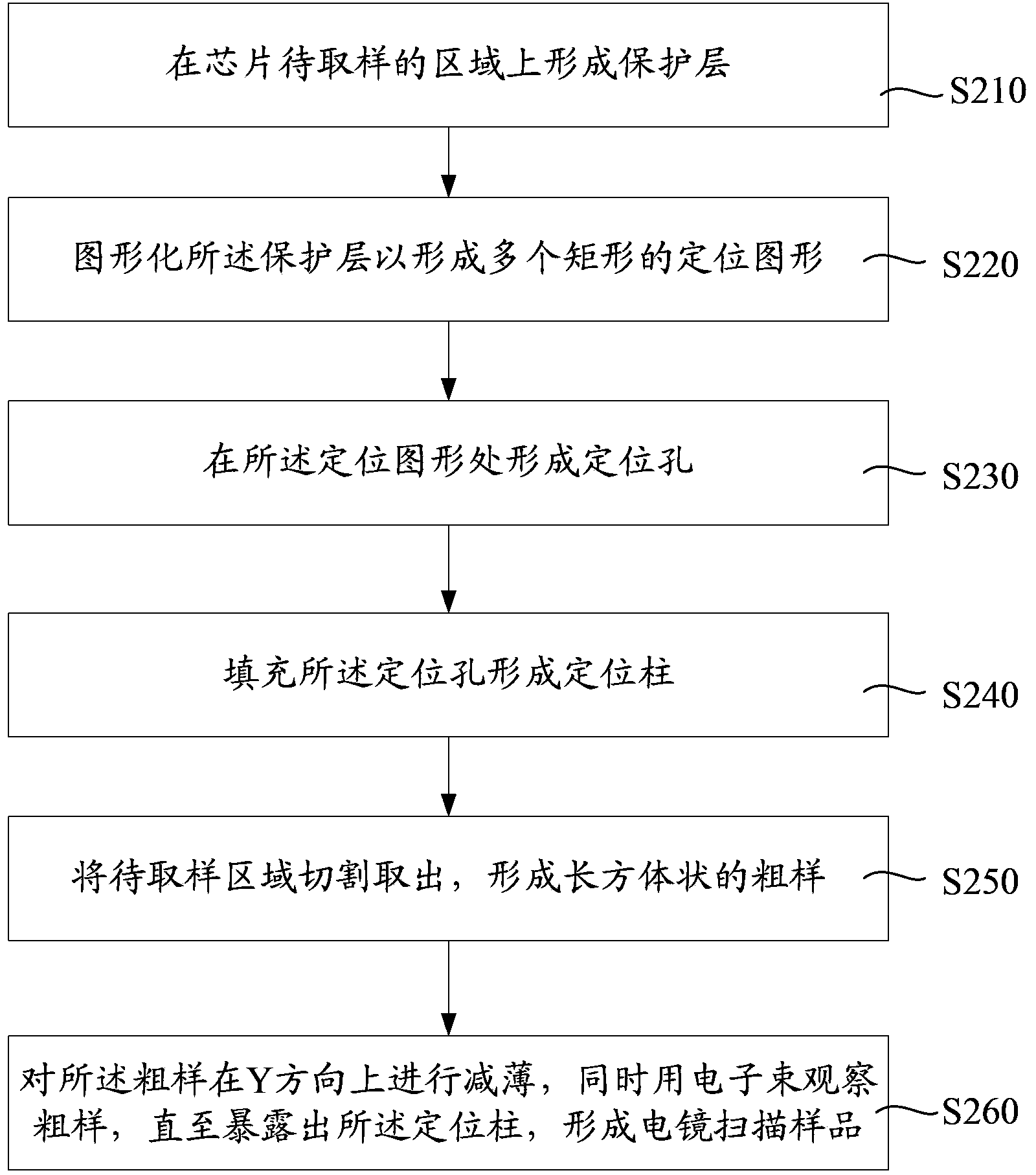
[0033] Please refer to figure 1 , which is a flowchart of the electron microscope scanning sample preparation method provided by the embodiment of the present invention, combined with the figure 1 , the method includes the following steps:

[0034] Step S210, forming a protective layer on the area of ​​the chip to be sampled;

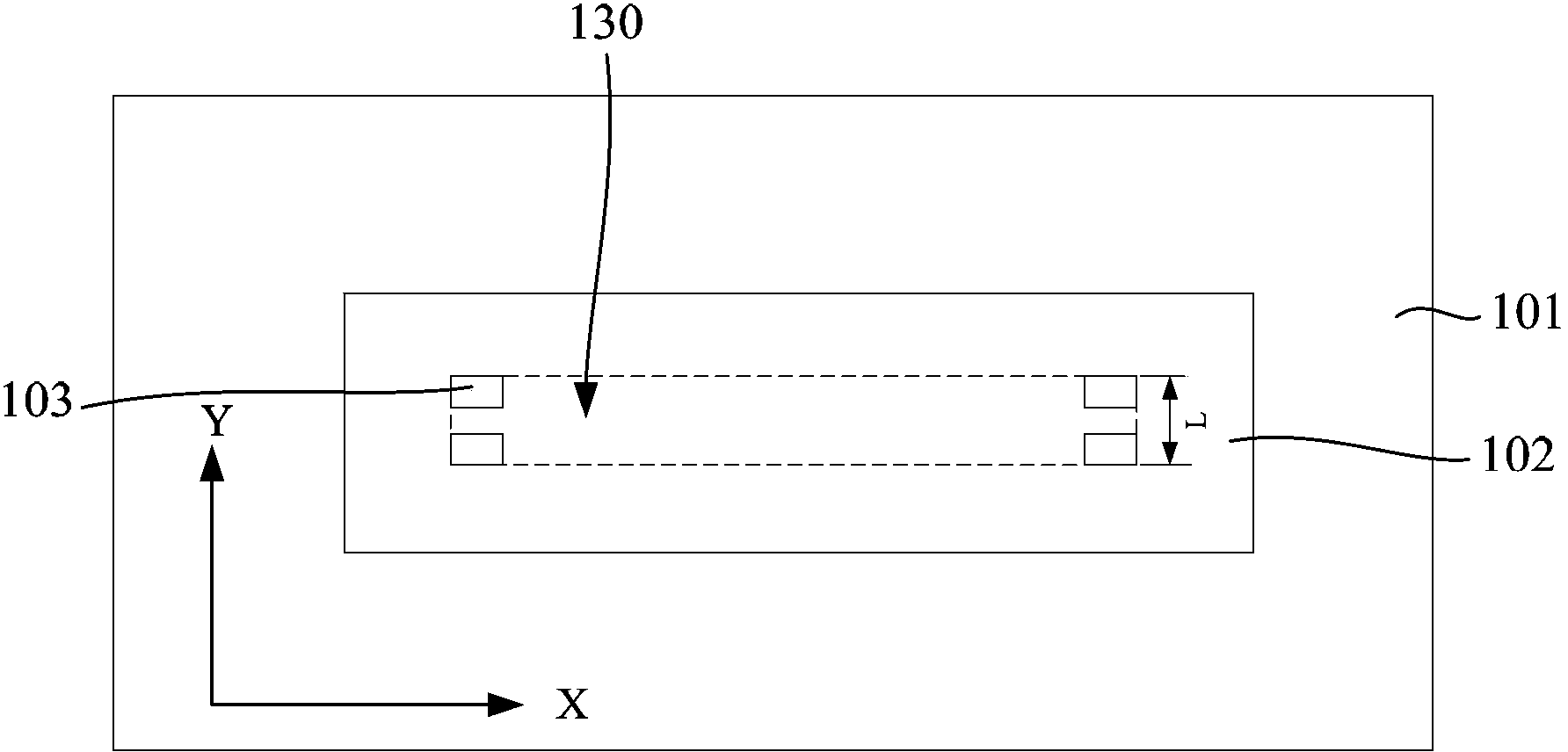
[0035] Step S220, patterning the protective layer to form a plurality of rectangular positioning patterns;

[0036] Step S230, forming a positioning hole at the positioning pattern;

[0037] Step S240, filling the positioning hole to form a positioning column;

[0038] Step S250, cutting out the area to be sampled to form a cuboid-shaped rough sample;

[0039] Step S260 , thinning the coarse sample in the Y direction, and observing the coarse sample with an electron beam until the positioning pillars are exposed to form a scanning electron microscope sample.

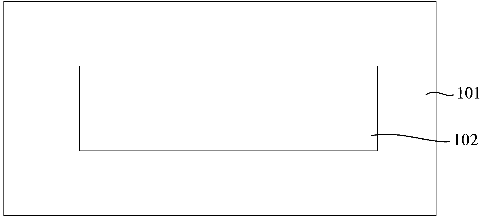
[0040] Wherein it is defined that the face where the protective layer is located is the t...


PUM

PropertyMeasurementUnit
lengthaaaaaaaaaa
lengthaaaaaaaaaa
lengthaaaaaaaaaa

Abstract

The invention discloses a preparation method of an electron microscope scanning sample, which comprises the following steps: forming a protective layer on a chip area to be sampled; imaging the protective layer to form positioning figures of several rectangles; forming a location hole on the positioning figure; filling the location hole to form a positioning column; cutting the area to be sampled and then taking out, forming a coarse sample in a cuboid shape; thinning the coarse sample along Y direction, observing the coarse sample by electron beam until the positioning column is exposed, and forming the electron microscope scanning sample. By controlling the sample thickness and thinning process of the positioning column, the sample thickness can be accurately controlled as the required thickness, and sample preparation time can be saved.

Description

technical field [0001] The invention relates to the fields of semiconductor manufacturing technology and material analysis, in particular to an electron microscope scanning sample preparation method. Background technique [0002] At present, with the continuous development of Moore's law, it is an effective method to take the stress of the channel region into consideration in the process of smaller and smaller line widths. NBD (Nano beam diffraction) is one of the effective methods to measure the stress distribution in the channel region so far, and it provides effective help for the research and development of stress in the process of advanced process development. [0003] In the prior art, NBD samples are usually prepared using FIB (Focus Ion Beam, focused ion beam). First, the sample to be processed is cut and taken out. At this time, the thickness of the sample does not reach the required thickness, and then it is thinned to the required thickness by FIB. Thickness, dur...

Claims


Application Information

Patent Timeline
Patent Type & Authority Applications(China)
IPC IPC(8): G01N1/28
Inventor 赵耀斌李日鑫戴海波于倩倩李会淑张彤刘文晓
Owner SEMICON MFG INT (SHANGHAI) CORP
Why Eureka
Try Eureka