touch screen

A touch screen and conductive layer technology, which is applied in lamination devices, instruments, electrical digital data processing, etc., can solve the problems of complicated production process, waste, and increased production cost, and achieve simple production process, low production cost and lower price Effect

Active Publication Date: 2018-01-12
ANHUI JINGZHUO OPTICAL DISPLAY TECH CO LTD
View PDF4 Cites 1 Cited by
  • Summary
  • Abstract
  • Description
  • Claims
  • Application Information

AI Technical Summary

Problems solved by technology

The preparation of the traditional ITO layer is generally to plate ITO on the glass, and obtain the required induction lines in the X and Y directions after etching. This traditional production process is complex and lengthy, and this production method inevitably requires engraving If the etching process is used, a large amount of ITO materials will be wasted, further increasing the manufacturing cost, making the price of the touch screen higher, resulting in a higher price of touch electronic products

Method used


Image

  • touch screen
  • touch screen
  • touch screen

Examples


preparation example Construction

[0046] The preparation of the above-mentioned UV-type photosensitive nano-conductive material is relatively simple, just mix the conductive agent, photosensitive material, photosensitive material and solvent according to a suitable ratio, and is convenient to use.

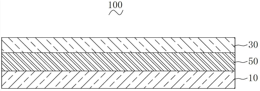
[0047] Preferably, the thickness of the first conductive electrode 32 is 0.01 micron to 15 micron, so that the light transmission of the first conductive layer is better.

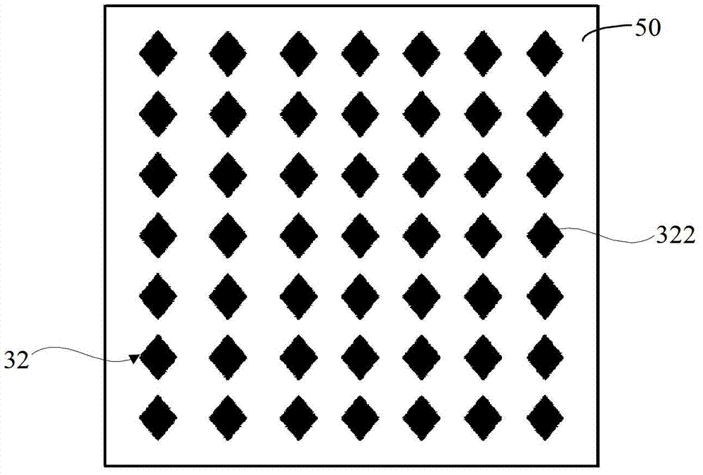
[0048] The first conductive electrode 32 includes a plurality of diamond-shaped conductive patterns 322 distributed in rows and columns. It can be understood that, in other implementation manners, the conductive pattern 322 may be in other shapes, such as square, rectangle, etc., or other irregular shapes.

[0049] A plurality of first conductive bridges are disposed on the first conductive electrode 32 , and each first conductive bridge connects the two connected conductive patterns 322 to conduct the two connected conductive patterns 322 .

...

Embodiment 1

[0067] Prepare touch screen

[0068] (1) Coating UV-type photosensitive nano-conductive material on one surface of the glass panel to form a UV-type photosensitive nano-conductive material layer with uniform thickness; on the UV-type photosensitive nano-conductive material layer covered with the required first conductive pattern nested mask plate, and then exposed, and then soak the exposed UV-type photosensitive nano-conductive material layer in an aqueous solution of sodium carbonate for development, after development and curing, the first conductive electrode is formed on the surface of the glass panel, Obtain a semi-finished product; wherein, the UV-type photosensitive nano-conductive material includes 0.6% of conductive agent, 10% of photosensitive material, 0.1% of photosensitive material and 89.3% of solvent in terms of mass percentage;

[0069] (2) Put the above semi-finished product into the automatic brushing machine, print photosensitive silver paste on the first co...

Embodiment 2

[0071] Prepare touch screen

[0072] (1) Coating UV-type photosensitive nano-conductive material on one surface of the glass panel to form a UV-type photosensitive nano-conductive material layer with uniform thickness; The nested mask plate is then exposed, and then the exposed UV-type photosensitive nano-conductive material layer is soaked in an aqueous solution of sodium bicarbonate for development, and after development and curing, the first conductive electrode is formed on the surface of the glass panel. Obtain a semi-finished product; wherein the UV-type photosensitive nano-conductive material includes 0.2% conductive agent, 15% photosensitive material, 0.8% photosensitive material and 84% solvent in terms of mass percentage;

[0073] (2) Put the above semi-finished product into the automatic brushing machine, print photosensitive silver paste on the first conductive electrode, put it into the infrared baking oven for pre-baking, and then put it into the exposure machine...


PUM

PropertyMeasurementUnit
thicknessaaaaaaaaaa

Abstract

The invention relates to a touch screen. The touch screen comprises a glass panel and an induction module which is arranged on the glass panel in a laminating mode; the induction module comprises a first conducting layer which is arranged on the glass panel; the first conducting layer comprises a first conducting electrode which is made of UV (Ultra Violet) type photoreceptive nanometer conducting materials and a plurality of first conducting bridges which are arranged on the first conducting electrode. According to the touch screen, the first conducting layer is made of the UV type photoreceptive nanometer conducting materials, UV type photoreceptive nanometer conducting ink coats the glass panel in a coating mode, then the first conducting electrode is produced in an exposure developing mode, finally silver paste prints the first conducting electrode to produce the plurality of first conducting bridges, the etching technology is saved due to the fact that ITO is replaced by UV type photoreceptive nanometer conducting materials, the production technology is simple, the production costs are low, and accordingly the price of the touch screen is low and reduction of the price of a touch electronic product is facilitated.

Description

technical field [0001] The invention relates to the technical field of touch, in particular to a touch screen. Background technique [0002] With the rapid development of the TP (TOUCPANEL) industry, there is an increasing demand for transparent conductive materials, but since the transparent conductive material commonly used in touch screens is indium tin oxide (ITO), the indium element in ITO is a rare and precious metal. Relative lack and high price make the price of touch electronic products higher. Therefore, it is urgent to find a new transparent conductive material to replace indium tin oxide (ITO), so as to reduce the price of touch electronic products. [0003] At present, ITO coating and ITO patterning are generally required to prepare touch screen electrodes with ITO. The preparation of the traditional ITO layer is generally to plate ITO on the glass, and obtain the required induction lines in the X and Y directions after etching. This traditional production pro...

Claims


Application Information

Patent Timeline
Patent Type & Authority Patents(China)
IPC IPC(8): G06F3/041B32B37/12
CPCG06F3/041G06F2203/04103
Inventor 周志华唐根初唐彬
Owner ANHUI JINGZHUO OPTICAL DISPLAY TECH CO LTD
Why Eureka
Try Eureka